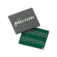
MT46H8M32LFB5-6:H Micron Technology Inc, MT46H8M32LFB5-6:H Datasheet - Page 65

MT46H8M32LFB5-6:H
Manufacturer Part Number
MT46H8M32LFB5-6:H
Description
IC SDRAM 256MB 166MHZ 90VFBGA
Manufacturer
Micron Technology Inc
Series
-r
Type
DDR SDRAMr
Specifications of MT46H8M32LFB5-6:H
Format - Memory
RAM
Memory Type
Mobile DDR SDRAM
Memory Size
256M (8Mx32)
Speed
166MHz
Interface
Parallel
Voltage - Supply
1.7 V ~ 1.95 V
Operating Temperature
0°C ~ 70°C
Package / Case
90-VFBGA
Organization
8Mx32
Density
256Mb
Address Bus
14b
Access Time (max)
6.5/5ns
Maximum Clock Rate
166MHz
Operating Supply Voltage (typ)
1.8V
Package Type
VFBGA
Operating Temp Range
0C to 70C
Operating Supply Voltage (max)
1.95V
Operating Supply Voltage (min)
1.7V
Supply Current
120mA
Pin Count
90
Mounting
Surface Mount
Operating Temperature Classification
Commercial
Lead Free Status / Rohs Status
Lead free / RoHS Compliant
Available stocks
Company
Part Number
Manufacturer
Quantity
Price
Company:
Part Number:
MT46H8M32LFB5-6:H
Manufacturer:
ST
Quantity:
34 600
Company:
Part Number:
MT46H8M32LFB5-6:H
Manufacturer:
Micron Technology Inc
Quantity:
10 000
Figure 28: READ-to-PRECHARGE
PDF: 09005aef834bf85b
256mb_mobile_ddr_sdram_t36n.pdf - Rev. I 09/10 EN
Command
Command
Address
Address
DQS
DQ
DQS
DQ
CK#
CK#
CK
CK
4
4
Notes:
Banka,
Col n
Banka,
Col n
READ
READ
T0
T0
1. BL = 4, or an interrupted burst of 8 or 16.
2. PRE = PRECHARGE command.
3. ACT = ACTIVE command.
4. D
5. Shown with nominal
6. READ-to-PRECHARGE equals 2 clocks, which enables 2 data pairs of data-out.
7. A READ command with auto precharge enabled, provided
1
1
cause a precharge to be performed at x number of clock cycles after the READ com-
mand, where x = BL/2.
OUT
n = data-out from column n.
CL = 2
NOP
NOP
T1
T1
CL = 3
T1n
T1n
(a or all)
(a or all)
D
t
Bank a,
Bank a,
AC,
OUT
n
T2
T2
PRE
PRE
t
2
65
2
DQSCK, and
D
n + 1
T2n
T2n
OUT
256Mb: x16, x32 Mobile LPDDR SDRAM
D
OUT
n
D
Micron Technology, Inc. reserves the right to change products or specifications without notice.
n + 2
T3
NOP
T3
NOP
OUT
t
DQSQ.
D
n + 1
Don’t Care
OUT
T3n
t
t
T3n
D
n + 3
RP
RP
OUT
D
n + 2
OUT
T4
T4
NOP
NOP
D
n + 3
OUT
t
RAS (MIN) is met, would
Transitioning Data
© 2008 Micron Technology, Inc. All rights reserved.
READ Operation
Bank a,
Bank a,
T5
T5
ACT
Row
ACT
Row
3
3


