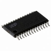
PCA9558PW,118 NXP Semiconductors, PCA9558PW,118 Datasheet - Page 14

PCA9558PW,118
Manufacturer Part Number
PCA9558PW,118
Description
IC I2C SMBUS 8BIT I/O 28TSSOP
Manufacturer
NXP Semiconductors
Datasheet
1.PCA9558PW112.pdf
(27 pages)
Specifications of PCA9558PW,118
Package / Case
28-TSSOP
Applications
PC's, PDA's
Interface
I²C
Voltage - Supply
3 V ~ 3.6 V
Mounting Type
Surface Mount
Logic Family
PCA9558
Number Of Lines (input / Output)
8.0 / 8.0
Propagation Delay Time
21 ns
Operating Supply Voltage
3 V to 3.6 V
Operating Temperature Range
0 C to + 70 C
Input Voltage
5 V
Logic Type
I2C, SMBus
Maximum Clock Frequency
400 KHz
Mounting Style
SMD/SMT
Number Of Input Lines
8.0
Number Of Output Lines
8.0
Output Voltage
5 V
Lead Free Status / RoHS Status
Lead free / RoHS Compliant
Lead Free Status / RoHS Status
Lead free / RoHS Compliant, Lead free / RoHS Compliant
Other names
935269433118
PCA9558PW-T
PCA9558PW-T
PCA9558PW-T
PCA9558PW-T
NXP Semiconductors
PCA9558_4
Product data sheet
Fig 17. Read from GPIO Input Port register and write to 256-byte EEPROM
S
START condition
1
See
0
slave address
Table 3
7.1.4.1 Power-on reset
7.1.4.2 External reset
0
7.1.4 Reset
1
7.2 Using the PCA9558 on the SMBus
1
for the needed command code.
1 A0 0
When the Write Protect (WP) input is a logic 0 it allows writes to both EEPROM arrays.
When it is a logic 1, it prevents any writes to the EEPROM arrays.
When power is applied to V
a reset state until V
the PCA9558 volatile registers and SMBus state machine will initialize to their default
states.
The GPIO outputs (IOx) will be selected as outputs.
The DIP switch MUX_OUTx and NON_MUXED_OUT pin values depend on:
A reset of the GPIO registers can be accomplished by holding the IO_OUT_LOW pin
LOW for a minimum of T
IO_OUT_LOW input is once again HIGH.
It is possible to use Intel chip sets to communicate with the PCA9558. There are no
limitations when the SMBus controller is communicating with the MUX or the GPIO;
however, there are limitations with the 2-kbit serial EEPROM. Because of being able to
address any location in the EEPROM block using the second command byte, the designer
using the PCA9558 on the SMBus will have to program around it, an easy thing to do. The
device designers had to deal with the specifics of addressing the EEPROM and chose the
I
EEPROM block.
In order to write to the EEPROM, write the EEPROM address byte in the Data0 byte and
the data to be sent should be placed in the Data1 byte. The Intel chip set’s Word Data
instruction would then send the address, followed by the command register then Data0
2
•
•
C-bus specification and use the second command byte to address any location in the
R/W
The MUX_OUT_LOW and MUX_SELECT logic levels
The previously stored values in the EEPROM register/current MUX_INx pin values as
shown in
A
acknowledge
from slave
0
Table 4
0
command byte
0
DD
1
has reached V
0
Rev. 04 — 14 April 2009
cy(W)
0
acknowledge
DD
from slave
1
. These GPIO registers return to their default states until the
, an internal Power-On Reset (POR) holds the PCA9558 in
0
A
POR
a7
a6 a5 a4 a3 a2 a1 a0
. At that point, the reset condition is released and
EEPROM address
GPIO input port data latched
acknowledge
from slave
8-bit I
A
programming begins after STOP
x
2
x x x x x x x
C-bus/SMBus I/O port
dummy byte
PCA9558
© NXP B.V. 2009. All rights reserved.
acknowledge
STOP condition;
from slave
002aad381
A
14 of 27
P


