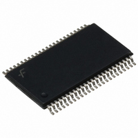
FIN1217MTD Fairchild Semiconductor, FIN1217MTD Datasheet - Page 8

FIN1217MTD
Manufacturer Part Number
FIN1217MTD
Description
IC SERIALIZER/DESERIALZR 48TSSOP
Manufacturer
Fairchild Semiconductor
Datasheet
1.FIN1215MTDX.pdf
(20 pages)
Specifications of FIN1217MTD
Function
Serializer/Deserializer
Data Rate
1.785Gbps
Input Type
LVTTL
Output Type
LVDS
Number Of Inputs
21
Number Of Outputs
3
Voltage - Supply
3 V ~ 3.6 V
Operating Temperature
-40°C ~ 85°C
Mounting Type
Surface Mount
Package / Case
48-TSSOP
Lead Free Status / RoHS Status
Lead free / RoHS Compliant
© 2003 Fairchild Semiconductor Corporation
FIN1215 / FIN1216 / FIN1217 • Rev. 1.0.3
Transmitter AC Electrical Characteristics
Typical values are at over supply voltages and operating temperatures ranges, unless otherwise specified.
Symbol
LVDS Transmitter Timing Characteristics
Transmitter Output Data Jitter (f=40 MHz)
Transmitter Output Data Jitter (f=65 MHz)
t
t
t
t
t
t
t
t
t
t
t
t
t
t
t
t
t
TPPB0
TPPB1
TPPB2
TPPB3
TPPB4
TPPB5
TPPB6
TPPB0
TPPB1
TPPB2
TPPB3
TPPB4
TPPB5
TPPB6
t
t
t
t
t
t
t
TPDD
TCCD
CLKT
t
t
TCP
TCH
TCL
TLH
THL
STC
HTC
XIT
JIT
Transmit Clock Period
Transmit Clock (TxCLKIn) HIGH Time
Transmit Clock LOW Time
TxCLKIn Transition Time (Rising and
Falling)
TxCLKIn Cycle-to-Cycle Jitter
TxIn Transition Time
Differential Output Rise Time (20% to 80%)
Differential Output Fall Time (80% to 20%)
TxIn Setup to TxCLNIn
TxIn Holds to TCLKIn
Transmitter Power-Down Delay
Transmitter Clock Input to Clock Output
Delay
Transmitter Output Pulse Position of Bit 0
Transmitter Output Pulse Position of Bit 1
Transmitter Output Pulse Position of Bit 2
Transmitter Output Pulse Position of Bit 3
Transmitter Output Pulse Position of Bit 4
Transmitter Output Pulse Position of Bit 5
Transmitter Output Pulse Position of Bit 6
Parameter
(12)
(12)
8
Figure 10
10% to 90%
Figure 11
Figure 8
Figure 10
f=85MHz FIN1217
only
Figure 17
Figure 13
T
Figure 20
Figure 20
a
a
A
=
=25°C, V
=
Conditions
f
f
×
1
×
1
7
7
(11)
CC
=3.3V
2a-0.25
3a-0.25
4a-0.25
5a-0.25
6a-0.25
a-0.25
2a-0.2
3a-0.2
4a-0.2
5a-0.2
6a-0.2
11.76
Min.
-0.25
a-0.2
0.35
0.35
-0.2
1.0
1.5
2.5
2.8
0
Continued on following page…
Typ.
0.50
0.50
0.75
0.75
5.5
2a
3a
4a
5a
6a
2a
3a
4a
5a
6a
T
0
a
0
a
2a+0.25
3a+0.25
4a+0.25
5a+0.25
6a+0.25
a+0.25
2a+0.2
3a+0.2
4a+0.2
5a+0.2
6a+0.2
50.00
a+0.2
Max.
0.65
0.65
1.50
1.50
0.25
100
6.0
3.0
6.0
6.8
0.2
www.fairchildsemi.com
Units
ns
ns
ns
ns
ns
ns
ns
ns
ns
ns
ns
ns
ns
ns
ns
ns
ns
ns
ns
ns
ns
ns
ns
ns
T
T


