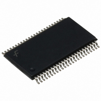
FIN1216MTDX Fairchild Semiconductor, FIN1216MTDX Datasheet - Page 18

FIN1216MTDX
Manufacturer Part Number
FIN1216MTDX
Description
IC SERIALIZER/DESERIAL 48-TSSOP
Manufacturer
Fairchild Semiconductor
Datasheet
1.FIN1215MTDX.pdf
(20 pages)
Specifications of FIN1216MTDX
Function
Serializer/Deserializer
Data Rate
1.785Gbps
Input Type
LVDS
Output Type
LVTTL
Number Of Inputs
3
Number Of Outputs
21
Voltage - Supply
3 V ~ 3.6 V
Operating Temperature
-40°C ~ 85°C
Mounting Type
Surface Mount
Package / Case
48-TSSOP
Lead Free Status / RoHS Status
Lead free / RoHS Compliant
Other names
FIN1216MTDX
FIN1216MTDXTR
FIN1216MTDXTR
Available stocks
Company
Part Number
Manufacturer
Quantity
Price
© 2003 Fairchild Semiconductor Corporation
FIN1215 / FIN1216 / FIN1217 • Rev. 1.0.3
AC Loadings and Waveforms
Note: t
Note: This jitter pattern is used to test the jitter response (clock out) of the device over the power supply range with
The minimum and maximum pulse position values are based on the bit position of each of the seven bits within
the LVDS data stream across PVT (Process, Voltage Supply, and Temperature).
worst jitter ±ns (cycle-to-cycle) clock input. The specific test methodology is as follows:
RSKM
is the budget for the cable skew and source clock skew plus Inter-Symbol Interference (ISI).
Switching input data TxIn0 to TxIn20 at 0.5MHz and the input clock is shifted to left -3ns and to
the right +3ns when data is HIGH (by switching between CLK1 and CLK2 in Figure 11).
The ±3ns cycle-to-cycle input jitter is the static phase error between the two clock sources.
Jumping between two clock sources to simulate the worst-case of clock edge jump (3ns) from
graphical controllers. Cycle-to-cycle jitter at TxCLK out pin should be measured cross V
with 100mV noise (V
Figure 22.
CC
noise frequency <2MHz).
(Continued)
Figure 23.
Receiver LVDS Input Skew Margin
18
Jitter Pattern
www.fairchildsemi.com
CC
range


