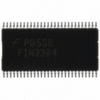
FIN3384MTDX Fairchild Semiconductor, FIN3384MTDX Datasheet - Page 18

FIN3384MTDX
Manufacturer Part Number
FIN3384MTDX
Description
IC SERIALIZER/DESERIAL 56-TSSOP
Manufacturer
Fairchild Semiconductor
Datasheet
1.FIN3384MTDX.pdf
(21 pages)
Specifications of FIN3384MTDX
Function
Serializer/Deserializer
Data Rate
2.38Gbps
Input Type
LVDS
Output Type
LVTTL
Number Of Inputs
4
Number Of Outputs
28
Voltage - Supply
3 V ~ 3.6 V
Operating Temperature
-10°C ~ 70°C
Mounting Type
Surface Mount
Package / Case
56-TSSOP
Lead Free Status / RoHS Status
Lead free / RoHS Compliant
Other names
FIN3384MTDX
FIN3384MTDXTR
FIN3384MTDXTR
© 2003 Fairchild Semiconductor Corporation
FIN3383/3384/3385/3386 • Rev. 1.0.4
AC Loadings and Waveforms
Note:
Note:
26. Test setup used considers no requirement for separation of RMS and deterministic jitter. Other hardware
27. This jitter pattern is used to test the jitter response (clock out) of the device over the power supply range with
28. Switching input data TxIn0 to TxIn20 at 0.5MHz and the input clock is shifted to left -3ns and to
29. The ±3ns cycle-to-cycle input jitter is the static phase error between the two clock sources. Jumping between
setup, such as Wavecrest boxes, can be used if no M1 software is available, but the test methodology in
Figure 24 should be followed.
worst jitter ±3ns (cycle-to-cycle) clock input. The specific test methodology is as follows:
the right +3ns when data is HIGH.
two clock sources to simulate the worst-case of clock-edge jump (3ns) from graphical controllers. Cycle-to-
cycle jitter at TxCLKOut pin should be measured cross V
<2MHz).
Figure 24. Timing Diagram of Transmitter Clock Input with Jitter
Figure 23. Transmitter Clock Out Jitter Measurement Setup
(Continued)
18
CC
range with 100mV noise (V
CC
noise frequency
www.fairchildsemi.com


