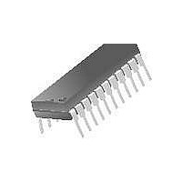
100322PC Fairchild Semiconductor, 100322PC Datasheet - Page 3

100322PC
Manufacturer Part Number
100322PC
Description
Buffers & Line Drivers 9-Bit Buffer
Manufacturer
Fairchild Semiconductor
Datasheet
1.100322PC.pdf
(6 pages)
Specifications of 100322PC
Logic Family
ECL
Logic Type
ECL
Number Of Channels Per Chip
9
Polarity
Non-Inverting
Supply Voltage (max)
- 5.7 V
Supply Voltage (min)
- 4.2 V
Maximum Operating Temperature
+ 85 C
Mounting Style
Through Hole
Package / Case
PDIP-24
High Level Output Current
- 50 mA
Minimum Operating Temperature
0 C
Number Of Lines (input / Output)
9 / 9
Propagation Delay Time
1.45 ns at - 4.2 V to - 5.7 V
Lead Free Status / Rohs Status
No
Available stocks
Company
Part Number
Manufacturer
Quantity
Price
Company:
Part Number:
100322PC
Manufacturer:
NS
Quantity:
6 239
t
t
t
t
t
t
t
t
V
V
V
V
V
V
I
I
I
t
t
t
t
PLH
PHL
TLH
THL
OSHL
OSLH
OST
PS
IL
IH
EE
PLH
PHL
TLH
THL
Commercial Version
PLCC AC Electrical Characteristics
V
Note 5: The propagation delay specified is for single output switching. Delays may vary up to 200 ps with multiple outputs switching.
Note 6: Output-to-Output Skew is defined as the absolute value of the difference between the actual propagation delay for any outputs within the same pack-
aged device. The specifications apply to any outputs switching in the same direction either HIGH to LOW (t
directions both HL and LH (t
Industrial Version
PLCC DC Electrical Characteristics
V
Note 7: The specified limits represent the “worst case” value for the parameter. Since these values normally occur at the temperature extremes, additional
noise immunity and guardbanding can be achieved by decreasing the allowable system operating ranges. Conditions for testing shown in the tables are cho-
sen to guarantee operation under “worst case” conditions.
PLCC AC Electrical Characteristics
V
Note 8: The propagation delay specified is for single output switching. Delays may vary up to 200 ps with multiple outputs switching.
OH
OL
OHC
OLC
IH
IL
Symbol
Symbol
Symbol
EE
EE
EE
4.2V to 5.7V, V
4.2V to 5.7V, V
4.2V to 5.7V, V
Propagation Delay
Data to Output
Transition Time
20% to 80%, 80% to 20%
Maximum Skew Common Edge
Output-to-Output Variation
Data to Output Path
Maximum Skew Common Edge
Output-to-Output Variation
Data to Output Path
Maximum Skew Opposite Edge
Output-to-Output Variation
Data to Output Path
Maximum Skew
Pin (Signal) Transition Variation
Data to Output Path
Output HIGH Voltage
Output LOW Voltage
Output HIGH Voltage
Output LOW Voltage
Input HIGH Voltage
Input LOW Voltage
Input LOW Current
Input HIGH Current
Power Supply Current
Propagation Delay
Data to Output
Transition Time
20% to 80%, 80% to 20%
Parameter
Parameter
Parameter
CC
CC
CC
OST
). Parameters t
V
V
V
CCA
CCA
CCA
GND
GND
GND, T
(Continued)
OST
C
and t
0.45
0.35
0.45
0.30
0.50
Min
Min
Min
1085
1830
1095
1170
1830
40 C to 85 C
65
PS
T
T
T
C
C
C
guaranteed by design.
0 C
40 C
40 C
Max
1.25
1.10
Max
1.25
1.20
200
200
260
200
Max
1575
1565
1480
300
870
870
30
(Note 7)
3
T
0.45
0.35
0.45
0.35
Min
Min
0.50
C
Min
1025
1830
1035
1830
1165
T
T
65
C
C
0 C to 85 C
25 C
25 C
Max
1.25
1.10
Max
1.25
1.10
200
200
260
200
Max
1620
1610
1475
240
870
870
30
0.45
0.35
0.45
0.35
Min
Min
Units
mV
mV
mV
mV
mA
T
T
OSHL
C
C
A
A
), or LOW to HIGH (t
85 C
85 C
V
or V
V
or V
Guaranteed HIGH Signal
for All Inputs
Guaranteed LOW Signal
for All Inputs
V
V
Inputs Open
Max
1.35
1.10
Max
1.35
1.10
200
200
260
200
IN
IN
IN
IN
IL (Min)
IL (Max)
V
V
V
V
IH (Max)
IH (Min)
IL (Min)
IH (Max)
Units
Units
www.fairchildsemi.com
Conditions
ns
ns
ps
ps
ps
ps
ns
ns
OSLH
), or in opposite
Figures 1, 2
(Note 5)
Figures 1, 2
(Note 6)
(Note 6)
(Note 6)
(Note 6)
Figures 1, 2
(Note 8)
Figures 1, 2
Conditions
Conditions
Loading with
50 to 2.0V
Loading with
50 to 2.0V


