KA348 Fairchild Semiconductor, KA348 Datasheet
KA348
Specifications of KA348


Related parts for KA348


KA348 Summary of contents
Page 1
... Internal Block Diagram ©2001 Fairchild Semiconductor Corporation www.fairchildsemi.com Description The KA248/KA348 is a true quad KA741. It consists of four independent, high gain, internally compensated, low power operational amplifiers which have been designed to provide functional characteristics identical to those of the familiar KA741 operational amplifier. In addition the total supply current for all four amplifiers is comparable to the supply current of a single KA741 type OP Amp ...
Page 2
... KA248/KA348 Schematic Diagram (One Section Only) Absolute Maximum Ratings Parameter Supply Voltage Differential Input Voltage Input Voltage Output Short Circuit Duration Operating Temperature KA248 KA348 Storage Temperature 2 Symbol Value I(DIFF Continuous +85 OPR 0~ + 65~ +150 STG Unit ...
Page 3
... Common Mode Input Voltage Range Small Signal Bandwidth Phase Margin (Note2) Slew Rate (Note2) Output Short Circuit Current Output Voltage Swing V Common Mode Rejection Ratio CMRR Power Supply Rejection Ratio Note : 1. KA348 + KA248: - Guaranteed by design. Conditions Min. Typ. Max. Min. Typ. Max. R 10K ...
Page 4
... KA248/KA348 Typical Performance Characteristics Supply Voltage (V) Figure 1. Supply Current vs Supply voltage Source Current (mA) Figure 3. Output voltage swing vs Source Current (mA) Frequency (Hz) Figure 5. Output Impedance vs Frequency 4 Supply Voltage (V) Figure 2. Output Voltage Swing vs Supply voltage Sink Current (mA) Figure 4. Output voltage swing vs Sink Current (mA) Frequency (Hz) Figure 6 ...
Page 5
... Typical Performance Characteristics (continued) Figure 7. Open Loop Frequency Response Figure 9. Large Signal Pulse Response Figure 11. Undistorted Output Voltage Swing vs Frequency Figure 8. Bode Plot Figure 10. Small Signal Pulse Response Figure 12. Inverting Large Signal Pulse Response KA248/KA348 5 ...
Page 6
... KA248/KA348 Typical Performance Characteristics (continued) Figure 13. Input Noise Voltage And Noise Current vs Fre- quency Figure 15. Negative Common.mode Input Voltage Limit vs Negative Supply Voltage 6 Figure 14. Positive Common Mode Input Voltage Limit vs Positiue Supply Voltage ...
Page 7
... Mechanical Dimensions Package 6.40 0.20 0.252 0.008 #1 #14 #7 7.62 0.300 14-DIP #8 3.25 0.20 0.128 0.008 5.08 MAX 0.200 KA248/KA348 0.20 MIN 0.008 3.30 0.30 0.130 0.012 7 ...
Page 8
... KA248/KA348 Mechanical Dimensions Package #1 #7 6.00 0.236 3.95 0.156 0.225 0.60 0.20 0.024 0.008 8 (Continued) 14-SOP 1.55 0.10 0.061 0.004 #14 #8 0.30 1.80 MAX 0.071 0.012 0.20 0.008 5.72 0.05 MIN 0.002 ...
Page 9
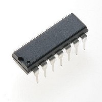
... Ordering Information Product Number Package KA348 14 DIP KA348D 14 SOP KA248 14 DIP KA248D 14 SOP Operating Temperature -25 ~ +85 C KA248/KA348 9 ...
Page 10
... KA248/KA348 DISCLAIMER FAIRCHILD SEMICONDUCTOR RESERVES THE RIGHT TO MAKE CHANGES WITHOUT FURTHER NOTICE TO ANY PRODUCTS HEREIN TO IMPROVE RELIABILITY, FUNCTION OR DESIGN. FAIRCHILD DOES NOT ASSUME ANY LIABILITY ARISING OUT OF THE APPLICATION OR USE OF ANY PRODUCT OR CIRCUIT DESCRIBED HEREIN; NEITHER DOES IT CONVEY ANY LICENSE UNDER ITS PATENT RIGHTS, NOR THE RIGHTS OF OTHERS. ...