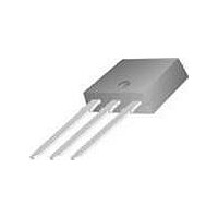
ISL9N315AD3 Fairchild Semiconductor, ISL9N315AD3 Datasheet

ISL9N315AD3
Specifications of ISL9N315AD3
Available stocks
Related parts for ISL9N315AD3
ISL9N315AD3 Summary of contents
Page 1
... ISL9N315AD3 / ISL9N315AD3ST N-Channel Logic Level PWM Optimized UltraFET General Description This device employs a new advanced trench MOSFET technology and features low gate charge while maintaining low on-resistance. Optimized for switching applications, this device improves the overall efficiency of DC/DC converters and allows operation to higher switching frequencies ...
Page 2
... 15V 10A 4.5V 10V 15V 10A 10V 2 23A 12A 23A, dI /dt = 100A 23A, dI /dt = 100A Min Typ Max 150 250 - - 100 0.012 0.015 - 0.022 0.028 - 900 - - 210 - - 9 15V DD = 23A - 1.0 1 1.0mA - 3 3 120 180 - - - - 1. 1 ISL9N315AD3/ISL9N315AD3ST Rev.A1 Units ...
Page 3
... C) Figure 2. Maximum Continuous Drain Current RECTANGULAR PULSE DURATION ( PULSE WIDTH (s) Figure 4. Peak Current Capability V = 10V 4. 100 125 150 175 CASE TEMPERATURE ( C) C Case Temperature NOTES: DUTY FACTOR PEAK FOR TEMPERATURES o ABOVE 25 C DERATE PEAK CURRENT AS FOLLOWS: 175 - 150 - ISL9N315AD3/ISL9N315AD3ST Rev. ...
Page 4
... 3.0V GS PULSE DURATION = 80 s DUTY CYCLE = 0.5% MAX 0.5 1.0 1.5 2 DRAIN TO SOURCE VOLTAGE (V) DS PULSE DURATION = 80 s DUTY CYCLE = 0.5% MAX V = 10V - 120 160 JUNCTION TEMPERATURE ( 250 120 160 JUNCTION TEMPERATURE ( C) J ISL9N315AD3/ISL9N315AD3ST Rev.A1 2.5 = 30A 200 200 ...
Page 5
... Figure 12. Gate Charge Waveforms for Constant 140 120 t f 100 80 t d(OFF d(ON Figure 14. Switching Time vs Gate Resistance DUT 0.01 Figure 16. Unclamped Energy Waveforms = 15V WAVEFORMS IN DESCENDING ORDER 30A 15A GATE CHARGE (nC) g Gate Currents = 10V 15V d(OFF d(ON GATE TO SOURCE RESISTANCE ( ) GS BV DSS ISL9N315AD3/ISL9N315AD3ST Rev. ...
Page 6
... Figure 17. Gate Charge Test Circuit Figure 19. Switching Time Test Circuit ©2003 Fairchild Semiconductor Corporation (Continued DUT g(REF) 0 Figure 18. Gate Charge Waveforms d(ON 90 DUT V GS 50% 10% 0 Figure 20. Switching Time Waveforms Q g(TOT g( g(TH OFF t d(OFF 10% 10% 90% 50% PULSE WIDTH ISL9N315AD3/ISL9N315AD3ST Rev.A1 = 10V 90% ...
Page 7
... 0.268 + Area ©2003 Fairchild Semiconductor Corporation , and the 125 application’s ambient 100 never exceeded (EQ 0. Figure 21. Thermal Resistance vs Mounting dissipation. Pulse values listed in the (EQ 33.32 + 23.84/(0.268+Area AREA, TOP COPPER AREA (in ) Pad Area ISL9N315AD3/ISL9N315AD3ST Rev.A1 10 ...
Page 8
... PSPICE Electrical Model .SUBCKT ISL9N315AD3 rev October 5.0e- 3.9e-10 CIN 6 8 7.8e-10 DBODY 7 5 DBODYMOD DBREAK 5 11 DBREAKMOD DPLCAP 10 5 DPLCAPMOD EBREAK 31.0 EDS EGS ESG EVTHRES EVTEMP LGATE GATE 1 LDRAIN 2 5 1.0e-9 RLGATE LGATE 1 9 4.53e-9 LSOURCE 3 7 5.38e-10 MMED MMEDMOD ...
Page 9
... SABER Electrical Model REV October 2002 template ISL9N315AD3 n2,n1,n3 electrical n2,n1,n3 { var i iscl dp..model dbodymod = (isl = 3.5e-11, nl=1.12 6.4e-3, trs1 = 1e-3, trs2 = 2e-6, xti=2.3, cjo = 6.1e-10 1e- 0.62) dp..model dbreakmod = (rs = 6e-1, trs1 = 1e-3, trs2 = -8.5e-6) dp..model dplcapmod = (cjo = 3.4e-10, isl=10e-30, nl=10, m=0.45) m ...
Page 10
... CTHERM6 2 tl 4.0e-2 RTHERM1 th 6 2.7e-3 RTHERM2 6 5 3.7e-3 RTHERM3 5 4 5.3e-2 RTHERM4 4 3 6.3e-1 RTHERM5 3 2 7.4e-1 RTHERM6 2 tl 7.6e-1 SABER Thermal Model SABER thermal model ISL9N315AD3T template thermal_model th tl thermal_c th ctherm.ctherm1 1.3e-3 ctherm.ctherm2 1.5e-3 ctherm.ctherm3 1.6e-3 ctherm.ctherm4 1.7e-3 ctherm.ctherm5 5.8e-3 ctherm ...
Page 11
... TRADEMARKS The following are registered and unregistered trademarks Fairchild Semiconductor owns or is authorized to use and is not intended exhaustive list of all such trademarks. ACEx™ FACT™ ActiveArray™ FACT Quiet Series™ ® Bottomless™ FAST CoolFET™ FASTr™ CROSSVOLT™ ...


