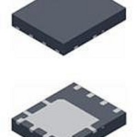
FDMS7620S Fairchild Semiconductor, FDMS7620S Datasheet

FDMS7620S
Specifications of FDMS7620S
Available stocks
Related parts for FDMS7620S
FDMS7620S Summary of contents
Page 1
... Thermal Resistance, Junction to Ambient θJA Package Marking and Ordering Information Device Marking Device FDMS7620S FDMS7620S ©2011 Fairchild Semiconductor Corporation FDMS7620S Rev.C1 ® MOSFET General Description = 10 This device includes two specialized MOSFETs in a unique dual = 7.5 A Power 56 package designed to provide an optimal synchro- D nous buck power stage in terms of efficiency and PCB utilization ...
Page 2
... Turn-Off Delay Time d(off) t Fall Time f Q Total Gate Charge g(TOT) Q Total Gate Charge g(TOT) Q Gate to Source Charge gs Q Gate to Drain “Miller” Charge gd ©2011 Fairchild Semiconductor Corporation FDMS7620S Rev. 25°C unless otherwise noted J Test Conditions = 250 μ mA 250 μA, referenced to 25° mA, referenced to 25° ...
Page 3
... Pulse Test: Pulse Width < 300 μs, Duty cycle < 2.0 N-ch device, the negative Vgs rating is for low duty cycle pulse ocurrence only. No continuous rating is implied based on starting Q2 based on starting ©2011 Fairchild Semiconductor Corporation FDMS7620S Rev. 25°C unless otherwise noted J Test Conditions 10 12.4 A ...
Page 4
... T J Figure 3. Normalized On Resistance vs Junction Temperature 27 μ PULSE DURATION = DUTY CYCLE = 0.5% MAX 150 1.5 2.0 2.5 3 GATE TO SOURCE VOLTAGE (V) GS Figure 5. Transfer Characteristics ©2011 Fairchild Semiconductor Corporation FDMS7620S Rev. 25°C unless otherwise noted 4 μ 3 2.0 2.5 3 100 125 150 0 - ...
Page 5
... Q , GATE CHARGE (nC) g Figure 7. Gate Charge Characteristics 125 J 1 0.001 0.01 0 TIME IN AVALANCHE (ms) AV Figure 9. Unclamped Inductive Switching Capability 1000 100 Figure 11. ©2011 Fairchild Semiconductor Corporation FDMS7620S Rev. 25°C unless otherwise noted J 1000 100 100 0. PULSE WIDTH (sec) Single Pulse Maximum Power Dissipation ...
Page 6
... Typical Characteristics (Q1 N-Channel) 2 DUTY CYCLE-DESCENDING ORDER 0.5 0.2 0.1 0.1 0.05 0.02 0.01 0.01 0.001 0.001 - Figure 12. ©2011 Fairchild Semiconductor Corporation FDMS7620S Rev. 25°C unless otherwise noted J SINGLE PULSE 125 C/W θ JA (Note 1b RECTANGULAR PULSE DURATION (sec) Junction-to-Ambient Transient Thermal Response Curve 6 ...
Page 7
... PULSE DURATION = 80 s DUTY CYCLE = 0.5% MAX 125 1.5 2.0 2 GATE TO SOURCE VOLTAGE (V) GS Figure 17. Transfer Characteristics ©2011 Fairchild Semiconductor Corporation FDMS7620S Rev. °C unless otherwise noted 3 μ s 1.5 2.0 Figure 14. Normalized on-Resistance vs Drain 50 75 100 125 150 - 0.01 0.001 3 ...
Page 8
... Q , GATE CHARGE (nC) g Figure 19. Gate Charge Characteristics 125 J 1 0.001 0.01 0 TIME IN AVALANCHE (ms) AV Figure 21. Unclamped Inductive Switching Capability 1000 100 ©2011 Fairchild Semiconductor Corporation FDMS7620S Rev. 25°C unless otherwise noted J 3000 1000 100 0. PULSE WIDTH (sec) Figure 23. Single Pulse Maximum Power ...
Page 9
... Typical Characteristics (Q2 N-Channel) 2 DUTY CYCLE-DESCENDING ORDER 0.5 0.2 0.1 0.1 0.05 0.02 0.01 0.01 0.001 - Figure 24. Junction-to-Ambient Transient Thermal Response Curve ©2011 Fairchild Semiconductor Corporation FDMS7620S Rev. °C unless otherwise noted J SINGLE PULSE 120 C/W θ JA (Note 1b RECTANGULAR PULSE DURATION (sec) 9 ...
Page 10
... FDMS7620S di/dt = 300 100 TIME (ns) Figure 25. FDMS7620S SyncFET body diode reverse recovery characteristic ©2011 Fairchild Semiconductor Corporation FDMS7620S Rev.C1 (continued) Schottky barrier diodes exhibit significant leakage at high tem- perature and high reverse voltage. This will increase the power in the device μ ...
Page 11
... Dimensional Outline and Pad Layout PIN#1 QUADRANT MAX 0.10 C 0.08 C 0.05 0.00 1 PIN #1 IDENT 0.66 0.55 0.340 0. 1.27 0.46 0. 0.05 C ©2011 Fairchild Semiconductor Corporation FDMS7620S Rev. (5X) TOP VIEW (0.20 ) SIDE VIEW SEATING PL ANE 2.67 0. 3.85 0.48 3.75 0.38 (5X) ...
Page 12
... Datasheet Identification Product Status Advance Information Formative / In Design Preliminary First Production No Identification Needed Full Production Obsolete Not In Production ©2011 Fairchild Semiconductor Corporation FDMS7620S Rev.C1 Power-SPM™ ® PowerTrench SM PowerXS™ Programmable Active Droop™ ® QFET QS™ Quiet Series™ RapidConfigure™ ...


