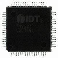
IDT82V1054APF IDT, Integrated Device Technology Inc, IDT82V1054APF Datasheet - Page 10

IDT82V1054APF
Manufacturer Part Number
IDT82V1054APF
Description
IC PCM CODEC 4CH MPI 3.3V 64TQFP
Manufacturer
IDT, Integrated Device Technology Inc
Type
Line Interface Units (LIUs)r
Datasheet
1.IDT82V1054APF8.pdf
(42 pages)
Specifications of IDT82V1054APF
Voltage - Supply
3.135 V ~ 3.465 V
Mounting Type
Surface Mount
Package / Case
64-TQFP, 64-VQFP
Lead Free Status / RoHS Status
Contains lead / RoHS non-compliant
Number Of Drivers/receivers
-
Protocol
-
Other names
82V1054APF
Available stocks
Company
Part Number
Manufacturer
Quantity
Price
Company:
Part Number:
IDT82V1054APF
Manufacturer:
IDT, Integrated Device Technology Inc
Quantity:
10 000
Company:
Part Number:
IDT82V1054APF8
Manufacturer:
IDT, Integrated Device Technology Inc
Quantity:
10 000
Company:
Part Number:
IDT82V1054APFG
Manufacturer:
IDT, Integrated Device Technology Inc
Quantity:
10 000
Company:
Part Number:
IDT82V1054APFG8
Manufacturer:
IDT, Integrated Device Technology Inc
Quantity:
10 000
IDT82V1054A QUAD PROGRAMMABLE PCM CODEC WITH MPI INTERFACE
2.1.2
channels. The digital PCM data can be compressed (A/
code. As shown in
as the Bit Clock (BCLK) or half of it. The PCM data is transmitted or
received either on the rising edges or on the falling edges of the BCLK
signal. The transmit and receive time slots can offset from the FS signal
by 0 to 7 periods of BCLK. All these configurations are made by global
register GREG7, which is effective for all four channels.
the PCM bus. The number of available time slots is determined by the
frequency of the BCLK signal. For example, if the frequency is 512 kHz,
8 time slots (TS0 to TS7) are available. If the frequency is 1.024 MHz,
16 time slots (TS0 to TS15) are available. The IDT82V1054A accepts
BCLK frequency of 512 kHz to 8.192 MHz at increments of 64 kHz.
of one channel occupies one time slot. The TT[6:0] bits in local register
LREG5 select the transmit time slot for each channel, while the RT[6:0]
bits in LREG6 select the receive time slot for each channel.
The IDT82V1054A provides two flexible PCM buses for all 4
The PCM data of each channel can be assigned to any time slot of
When compressed PCM code (8-bit wide) is selected, the voice data
When linear PCM code is selected, the voice data is a 16-bit 2’s
PCM BUS
Figure -
Single Clock
Double Clock
3, the data rate can be configured as same
BCLK
BCLK
FS
Figure - 3 Sampling Edge Selection Waveform
Bit 7
TS0
µ
-law) or linear
10
complement number (b13 to b0 are effective bits, b15 and b14 are as
same as the sign bit b13). So, the voice data of one channel occupies
one time slot group, which consists of 2 adjacent time slots. The TT[6:0]
bits in LREG5 select a transmit time slot group for the specified channel.
If TT[6:0] = n(d), it means that time slots TS(2n+1) and TS(2n+2) are
selected. For example, if TT[6:0] = 00H, it means that TS0 and TS1 are
selected. The RT[6:0] bits in LREG6 select a receive time slot group for
the specified channel in the same way.
transmit PCM highway one (DX1) or two (DX2) on the programmed
edges of BCLK according to time slot assignment. The transmit PCM
highway is selected by the THS bit in LREG5. The frame sync (FS)
pulse identifies the beginning of a transmit frame (TS0). The PCM data
is serially transmitted on DX1 or DX2 with MSB first.
PCM highway one (DR1) or two (DR2) on the programmed edges of
BCLK according to time slot assignment. The receive PCM highway is
selected by the RHS bit in LREG6. The frame sync (FS) pulse identifies
the beginning of a receive frame (TS0). The PCM data is serially
received from DR1 or DR2 with MSB first.
The PCM data of each individual channel can be clocked out to
The PCM data of each individual channel is received from receive
PCM Clock Slope Bits
CS = 000
CS = 001
CS = 010
CS = 011
CS = 100
CS = 101
CS = 110
CS = 111
in GREG7:
Transmit
Receive
INDUSTRIAL TEMPERATURE


