FAN3278TMX Fairchild Semiconductor, FAN3278TMX Datasheet - Page 3
FAN3278TMX
Manufacturer Part Number
FAN3278TMX
Description
MOSFET & Power Driver ICs Low-Voltage 27V PMOS NMOS Bridge Driver
Manufacturer
Fairchild Semiconductor
Datasheet
1.FAN3278TMX.pdf
(15 pages)
Specifications of FAN3278TMX
Product
MOSFET Gate Drivers
Rise Time
17 ns
Fall Time
8 ns
Propagation Delay Time
45 ns
Supply Voltage (max)
27 V
Supply Current
1.3 mA
Mounting Style
SMD/SMT
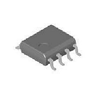
Package / Case
SOIC-8
Output Current
1.5 A
Output Voltage
30 V
Lead Free Status / Rohs Status
Lead free / RoHS Compliant
Available stocks
Company
Part Number
Manufacturer
Quantity
Price
Company:

Part Number:
FAN3278TMX
Manufacturer:
PANASONIC
Quantity:
12 000
Part Number:
FAN3278TMX
Manufacturer:
FAIRCHILD/仙童
Quantity:
20 000


© 2010 Fairchild Semiconductor Corporation
FAN3278 • Rev. 1.0.0
Pin Configuration
Thermal Characteristics
Notes:
1.
2.
3.
4.
5.
6.
Pin Definitions
Pin#
1
8
3
2
4
7
5
6
Estimates derived from thermal simulation; actual values depend on the application.
Theta_JL (
(including any thermal pad) that are typically soldered to a PCB.
Theta_JT (
assuming it is held at a uniform temperature by a top-side heatsink.
Theta_JA (Θ
and airflow. The value given is for natural convection with no heatsink using a 2S2P board, as specified in
JEDEC standards JESD51-2, JESD51-5, and JESD51-7, as appropriate.
Psi_JB (
temperature and an application circuit board reference point for the thermal environment defined in Note 4. For
the SOIC-8 package, the board reference is defined as the PCB copper adjacent to pin 6.
Psi_JT (
temperature and the center of the top of the package for the thermal environment defined in Note 4.
8-Pin Small-Outline Integrated Circuit (SOIC)
Name
OUTB
OUTA
GND
ENA
ENB
VDD
INA
INB
JT
JB
): Thermal characterization parameter providing correlation between the semiconductor junction
): Thermal characterization parameter providing correlation between semiconductor junction
JL
JT
JA
): Thermal resistance between the semiconductor junction and the bottom surface of all the leads
): Thermal resistance between the semiconductor junction and the top surface of the package,
): Thermal resistance between junction and ambient, dependent on the PCB design, heat sinking,
Enable Input for Channel A. Pull pin LOW to inhibit driver A. ENA has TTL thresholds.
Enable Input for Channel B. Pull pin LOW to inhibit driver B. ENB has TTL thresholds.
Ground. Common ground reference for input and output circuits.
Input to Channel A.
Input to Channel B.
Gate Drive Output A: Held LOW unless required input is present and V
voltage threshold where the IC is functional.
Gate Drive Output B (inverted from the input). Held HIGH unless the required input is present
and V
Supply Voltage. Provides power to the IC.
Package
DD
is above the internal voltage threshold where the IC is functional.
(1)
Figure 3. Pin Configuration (Top View)
3
Description
40
JL
(2)
JT
31
(3)
JA
89
(4)
DD
JB
43
is above the internal
(5)
JT
3
(6)
www.fairchildsemi.com
Unit
°C/W
Related parts for FAN3278TMX
Image
Part Number
Description
Manufacturer
Datasheet
Request
R

Part Number:
Description:
The FAN3278 dual 1
Manufacturer:
Fairchild Semiconductor
Datasheet:
Part Number:
Description:
Fairchild Semiconductor [IGBT MODULE]
Manufacturer:
Fairchild Semiconductor
Datasheet:

Part Number:
Description:
Discrete Semiconductor Modules
Manufacturer:
Fairchild Semiconductor
Part Number:
Description:
Discrete Semiconductor Modules
Manufacturer:
Fairchild Semiconductor
Part Number:
Description:
This N-Channel MOSFET is produced using Fairchild Semiconductor’s advanced Power Trench® process
Manufacturer:
Fairchild Semiconductor
Datasheet:
Part Number:
Description:
This N-Channel MOSFET is produced using Fairchild Semiconductor’s advanced Power Trench® process
Manufacturer:
Fairchild Semiconductor
Datasheet:
Part Number:
Description:
This N-Channel MOSFET is produced using Fairchild Semiconductor’s advanced PowerTrench® process
Manufacturer:
Fairchild Semiconductor
Datasheet:
Part Number:
Description:
This N-Channel MOSFET is produced using Fairchild Semiconductor’s advanced PowerTrench® process
Manufacturer:
Fairchild Semiconductor
Datasheet:
Part Number:
Description:
This N-Channel MOSFET is produced using Fairchild Semiconductor’s advanced Power Trench® process
Manufacturer:
Fairchild Semiconductor
Datasheet:
Part Number:
Description:
This N-Channel logic Level MOSFETs are produced using Fairchild Semiconductor‘s advanced Power Trench® process that has been special tailored to minimize the on-state resistance and yet maintain superior switching performance
Manufacturer:
Fairchild Semiconductor
Datasheet:
Part Number:
Description:
This N-Channel MOSFET is produced using Fairchild Semiconductor’s advanced Power Trench® process
Manufacturer:
Fairchild Semiconductor
Datasheet:
Part Number:
Description:
This N-Channel SyncFET™ is produced using Fairchild Semiconductor’s advanced PowerTrench® process
Manufacturer:
Fairchild Semiconductor
Datasheet:
Part Number:
Description:
This N-Channel SyncFET™ is produced using Fairchild Semiconductor’s advanced PowerTrench® process
Manufacturer:
Fairchild Semiconductor
Datasheet:
Part Number:
Description:
This N-Channel SyncFET™ is produced using Fairchild Semiconductor’s advanced PowerTrench® process
Manufacturer:
Fairchild Semiconductor
Datasheet:
Part Number:
Description:
This N-Channel logic Level MOSFETs are produced using Fairchild Semiconductor‘s advanced Power Trench® process that has been special tailored to minimize the on-state resistance and yet maintain superior switching performance
Manufacturer:
Fairchild Semiconductor
Datasheet: