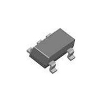
ILC7071AIM525X Fairchild Semiconductor, ILC7071AIM525X Datasheet - Page 8

ILC7071AIM525X
Manufacturer Part Number
ILC7071AIM525X
Description
Low Dropout (LDO) Regulators 0.10A LDO
Manufacturer
Fairchild Semiconductor
Datasheet
1.ILC7071AIM533X.pdf
(11 pages)
Specifications of ILC7071AIM525X
Number Of Outputs
1
Polarity
Positive
Input Voltage Max
0.6 V
Output Voltage
2.5 V
Output Type
Fixed
Dropout Voltage (max)
320 V
Output Current
0.15 A
Line Regulation
0.075 % / V
Load Regulation
0.25 %
Voltage Regulation Accuracy
1 %
Maximum Power Dissipation
150 mW
Maximum Operating Temperature
+ 85 C
Mounting Style
SMD/SMT
Package / Case
SOT-23
Minimum Operating Temperature
- 40 C
Lead Free Status / Rohs Status
Lead free / RoHS Compliant
ILC7071
Application Information
Capacitor Selection
In general, ceramic capacitors are preferred due to their
superior ESR performance. Those with X5R dielectric offer
the best temperature coefficient.
An input capacitor of 1µF or greater, connected between
Input and Ground, located in close proximity to the device
will improve the transient response and the noise rejection.
An output capacitor of at least 1µF is required to maintain
regulator loop stability. Stable operation will be achieved
with a wide variety of capacitors with ESR ranging from
10mΩ to 10Ω.
An optional capacitor connected between the CN pin and
ground can significantly reduce noise on the output.Values
ranging up to 10nF can be used, depending upon the sensi-
tivity to output noise in the application. Care should be taken
to prevent noise from external sources to enter into the CN
pin, which is a very sensitive, high impedance pin. Leakage
currents into this pin will directly affect the regulator accu-
racy and should be kept as low as possible.
Control Functions
Enable Pin
Applying a voltage of 0.6V or less at the Enable pin will
disable the output, reducing the quiescent output current to
less than 1µA, while a voltage of 2V or greater will enable
the device. If this shutdown function is not needed, the pin
can simply be connected to the V
float will cause erratic operation.
Thermal Protection
The ILC7071 is designed to supply high peak output currents
for brief periods, however this output load will cause the
device temperature to increase and exceed maximum ratings
due to power dissipation. During output overload conditions,
when the die temperature exceeds the shutdown limit tem-
perature of 125 °C, onboard thermal protection will disable
the output until the temperature drops below this limit,at
which point the output is then re-enabled.
During a thermal shutdown situation the user may assert the
power-down function at the Enable pin, reducing power
consumption to the minimum level.
8
IN
pin. Allowing this pin to
Thermal Characteristics
The ILC7071 is designed to supply up to 100mA at the
specified output voltage with an operating die (junction)
temperature of up to 125 °C. While the power dissipation is
calculated from known electrical parameters, the thermal
resistance is a result of the thermal characteristics of the
compact SOT-23-5 surface-mount package and the surround-
ing PC Board copper to which it is mounted.
The relationship describing the thermal behavior of the pack-
age is:
where T
ture of the die, which is 125 °C, and TA is the ambient
operating temperature. Θ
PC board layout and can be empirically obtained. While the
Θ
at 130 °C/W, the Θ
at least 235 °C/W.
This can be improved upon by providing a heat sink of
surrounding copper ground on the PCB.
Depending on the size of the copper area, the resulting Θ
can range from approximately 180 °C/W for one square
inch, to nearly 130 °C/W for 4 square inches.
The addition of backside copper with through-holes, stiffen-
ers, and other enhancements can also aid in reducing this
value. The heat contributed by the dissipation of other
devices located nearby must be included in design consider-
ations.
Once the limiting parameters in the thermal relationship
have been determined, the electrical design should be
verified to ensure that the device remains within specified
operating conditions.
If overload conditions are not considered, it is possible for
the device to enter a thermal cycling loop, in which the
circuit enters a shutdown condition, cools, reenables, and
then again overheats and shuts down repeatedly due to an
unmanaged fault condition.
JC
P
(junction-to-case) of the SOT-23-5 package is specified
D max
(
J(max)
)
=
is the maximum allowable junction tempera-
T
--------------------------------
J max
(
JA
Θ
JA
of the minimum PWB footprint will be
)
–
T
JA
A
is dependent on the surrounding
PRODUCT SPECIFICATION
REV. 1.0.2 7/16/03
JA


