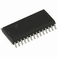
SCANPSC100FSCX Fairchild Semiconductor, SCANPSC100FSCX Datasheet

SCANPSC100FSCX
Specifications of SCANPSC100FSCX
Related parts for SCANPSC100FSCX
SCANPSC100FSCX Summary of contents
Page 1
... Small Outline Integrated Circuit (SOIC), JEDEC MS-013, 0.300 Wide Devices also available in Tape and Reel. Specify by appending the suffix letter “X” to the ordering code. Connection Diagram FACT is a trademark of Fairchild Semiconductor Corporation. © 2000 Fairchild Semiconductor Corporation Features Compatible with IEEE Std. 1149.1 (JTAG) Test Access Port and Boundary Scan Architecture Supported by Fairchild’ ...
Page 2
Pin Descriptions Pin Name RST (Input) The Reset pin is an asynchronous input that, when LOW, initializes the SCANPSC100. Mode bits, Shifter/Buffer and CNT32 control logic, TCK Control, and the PPI are all initialized to defined states. RST has hysteresis ...
Page 3
Chip Architecture The SCANPSC100 is designed to act together with a paral- lel bus host as a serial test bus master. Parallel data is writ- ten by the host to the SCANPSC100, which serializes the data for application to a ...
Page 4
Mode and Status Registers MODE REGISTER 0 (MODE0) Bit 7 Bit 6 Bit 5 TDO TDI CNT32 Enable Enable Enable This register is purely a mode register. All bits are writable and readable. The value 00100000 is placed in this ...
Page 5
Mode and Status Registers MODE REGISTER 2 (MODE2) Write: Bit 7 Bit 6 Bit 5 Not Not Not Used Used Used Read: Bit 7 Bit 6 Bit 5 TDO TDI CNT32 Status Status Status This register contains both mode and ...
Page 6
Parallel Processor Interface (PPI) TIMING WAVEFORMS Note 1: Valid data is provided on the RDY line a t after R/W is asserted LOW PD1 until the addressed register is ready to participate in the write operation. This ...
Page 7
Parallel Processor Interface (PPI) TIMING WAVEFORMS (Continued) FIGURE 4. Consecutive Read/Writes (best case timing) FIGURE 5. Consecutive Read/Writes (worst case timing) Note 3: Figures 4, 5: Figure 4 shows the best case bus cycle timing for SCK and STB during ...
Page 8
Parallel Processor Interface (PPI) READ AND WRITE CYCLES A Write cycle (see Figure 2) is initiated by asserting CE and R/W low followed by a LOW on STB a set time later. CE and STB are gated within the PSC100F ...
Page 9
Parallel Processor Interface (PPI) MODE1(7) 1 and TDO MODE1(6) Shifter/Buffer Not Full Shifter/Buffer Not Empty Note 6: Interrupts are generated using the INT pin. Three events trigger INT HIGH. Each event has its own mode bit ...
Page 10
Serial Scan Interface (SSI) TCK CONTROL TCK CONTROL is the central control block that enables or disables shift operations and provides byte alignment for the shifter/buffers. The state of all shifter/buffers and the 32-bit counter (CNT32) is evaluated here and ...
Page 11
Serial Scan Interface (SSI) TMS(1:0) SHIFTER/BUFFERS The TMS Shifter/Buffer block diagram is shown in Figure 10. These two blocks take parallel data and serialize it for shift operations through the serial port pins TMS0 and TMS1. Double-buffering is achieved by ...
Page 12
Serial Scan Interface (SSI) FIGURE 11. TDO Shifter/Buffer Block Diagram Register Hookup FIGURE 12. TDO PRPG Block Diagram The PRPG is loaded by four PPI writes to the TDO address. When the PRPG enable bit is set, a pulse is ...
Page 13
Serial Scan Interface (SSI) bits. This will assure that the desired bits will be accurately shifted to the boundary scan chain. For example, moving the TAP controllers within the boundary scan chain con- nected to TMS0 from the Pause-DR state ...
Page 14
Serial Scan Interface (SSI) FIGURE 13. TDI Shifter/Buffer Block Diagram FIGURE 14. TDI SSC Block Diagram SSC MODE. By setting MODE1(3), the TDI Shifter/Buffer is reconfigured as a 16-bit SSC (Serial Signature Compac- tor) using the primitive polynomial ...
Page 15
Serial Scan Interface (SSI) controllers within the scan chain(s) must be considered when developing Loop-Back test vectors to prevent undes- ired shifting of data or TAP controller transitions within the scan chain. 32-BIT COUNTER (CNT32) CNT32 is a 32-bit, count-down ...
Page 16
Application Note SCK MINIMUM PULSE WIDTH CALCULATION The SCANPSC100 Parallel to Serial Converter is intended to act as the interface between a processor and an IEEE 1149.1 boundary scan chain. When used in this configura- tion, there is a critical ...
Page 17
PROGRAMMING RESTRICTIONS Note Minimize the lengths of these two traces. FIGURE 17. SCANPSC100 Location Relative to Targets (Continued) 17 www.fairchildsemi.com ...
Page 18
Absolute Maximum Ratings Supply Voltage ( Input Diode Current ( 0. 0. Input Voltage ( Output Diode Current ( ...
Page 19
DC Electrical Characteristics V CC Symbol Parameter (V) I Maximum Quiescent CCMAX 5.5 Supply Current I Maximum CCT 5.5 I /Input CC I Maximum CCTR I /Input 5 Dynamic Power CCD Supply Current 5.5 (Note 8) Note 8: ...
Page 20
AC Electrical Characteristics/Operating Requirements V CC Symbol Parameter (V) (Note 9) t Clock Pulse Width 5.0 W SCK (L) SCK (H) t Pulse Width W1 5.0 STB ( Maximum MAX 5.0 Frequency Clock SERIAL SCAN INTERFACE (SSI) ...
Page 21
Physical Dimensions inches (millimeters) unless otherwise noted 28-Lead Small Outline Integrated Circuit (SOIC), JEDEC MS-013, 0.300 Wide Fairchild does not assume any responsibility for use of any circuitry described, no circuit patent licenses are implied and Fairchild reserves the right ...


