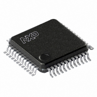
TDA8007BHL/C3,118 NXP Semiconductors, TDA8007BHL/C3,118 Datasheet - Page 40

TDA8007BHL/C3,118
Manufacturer Part Number
TDA8007BHL/C3,118
Description
IC INTERFACE CARD MP 48-LQFP
Manufacturer
NXP Semiconductors
Datasheet
1.TDA8007BHLC3118.pdf
(51 pages)
Specifications of TDA8007BHL/C3,118
Controller Type
Multiprotocol IC Card Interface
Interface
Parallel
Voltage - Supply
2.7 V ~ 6 V
Current - Supply
315mA
Operating Temperature
-40°C ~ 85°C
Mounting Type
Surface Mount
Package / Case
48-LQFP
Maximum Operating Temperature
+ 85 C
Minimum Operating Temperature
- 40 C
Mounting Style
SMD/SMT
Lead Free Status / RoHS Status
Lead free / RoHS Compliant
Other names
568-3520-2
935272525118
TDA8007BHLBE-T
935272525118
TDA8007BHLBE-T
Available stocks
Company
Part Number
Manufacturer
Quantity
Price
Company:
Part Number:
TDA8007BHL/C3,118
Manufacturer:
NXP Semiconductors
Quantity:
10 000
NXP Semiconductors
Table 35.
V
[1]
[2]
[3]
[4]
12. Timings
Table 36.
V
TDA8007BHL
Product data sheet
Symbol
t
Configured as output
V
V
t
Interrupt line: pin INT (open-drain output)
V
I
Symbol
Timing for non-multiplexed bus
Read control; see
t
t
t
Write control; see
t
t
t
t
Timing for bit CRED
Read operations in UART receive register; see
t
t
t
t
Write operations in UART transmit register; see
t
t
Write operations in time-out configuration register; see
t
i(r)
o(r)
LIH
1
2
3
4
5
6
7
W(RD)
RD(URR)
SB(FE)
SB(RBF)
W(WR)
WR(UTR)
W(WR)
DD
DD
OL
OH
OH
, t
, t
= 3.3 V; V
To meet these specifications, two ceramic multilayer capacitors with low ESR of minimum 100 nF should be used.
Pin I/O1 has an integrated 14 kΩ pull-up resistance to V
Pins C41 and C81 have an integrated 10 kΩ pull-up resistance to V
resistance to V
Pin I/OAUX has a 14 kΩ pull-up resistance to V
= 3.3 V; V
i(f)
o(f)
Parameter
input transition time (rise and fall time) C
low-level output voltage
high-level output voltage
output transition time (rise and fall
time)
low-level output voltage
high-level input leakage current
Characteristics
Timings
Parameter
RD high to CS low
access time CS low to data out valid
CS high to data out (high)
data valid to end-of-write
data hold time
RD low to CS or WR low
address stable to CS or WR high
RD pulse width
RD low to bit CRED = 1
set bit time FE
set time bit RBF
WR pulse width
WR pulse width
WR low to I/O low
DDA
DDA
CC2
= 3.3 V; T
= 3.3 V; T
Figure 5
Figure 4
.
and
amb
amb
…continued
6
= 25 °C; unless otherwise specified.
= 25°C; unless otherwise specified.
All information provided in this document is subject to legal disclaimers.
DD
Figure 9
Figure 10
.
Rev. 8 — 11 January 2011
Conditions
Conditions
I
I
C
I
OL
OH
OH
L
L
CC1
= 30 pF
= 30 pF
Figure 11
= 1 mA
= 40 mA
= 2 mA
and pin I/O2 has an integrated 14 kΩ pull-up resistance to V
CC1
and pins C42 and C82 have an integrated 10 kΩ pull-up
Min.
10
-
-
10
10
10
10
10
t
10.5
10.5
10
t
10
W(RD)
W(WR)
+ 2T
+ 2T
cy(CLK)
cy(CLK)
-
Min
-
-
0.75V
-
-
Multiprotocol IC card interface
Typ.
-
-
-
-
-
-
-
-
-
-
-
-
-
-
TDA8007BHL
DD
Max.
-
50
10
-
-
-
-
-
t
-
-
-
t
-
Typ
-
-
-
-
-
-
W(RD)
W(WR)
© NXP B.V. 2011. All rights reserved.
+ 3T
+ 3T
Max
1.2
300
V
0.1
0.3
10
DD
cy(CLK)
cy(CLK)
+ 0.25 V
CC2
.
40 of 51
Unit
ns
ns
ns
ns
ns
ns
ns
ns
ns
ETU
ETU
ns
ns
ns
Unit
µs
mV
µs
V
µA


