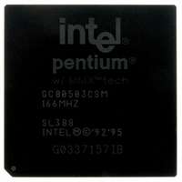
GC80503CSM66166SL388 Intel, GC80503CSM66166SL388 Datasheet - Page 9

GC80503CSM66166SL388
Manufacturer Part Number
GC80503CSM66166SL388
Description
IC MPU 1.9V PENTI 166MHZ 352BGA
Manufacturer
Intel
Datasheet
1.GC80503CSM66166SL388.pdf
(62 pages)
Specifications of GC80503CSM66166SL388
Rohs Status
RoHS non-compliant
Processor Type
Pentium I w/MMX
Features
66MHz Bus
Speed
166MHz
Voltage
1.9V
Mounting Type
Surface Mount
Package / Case
352-BGA
Other names
821225
2.1
Datasheet
Pentium
The application instruction set of the Pentium processor family includes the complete Intel486
CPU family instruction set with extensions to accommodate some of the additional functionality of
the Pentium processors. All application software written for the Intel386 and Intel486 family
microprocessors will run on the Pentium processors without modification. The on-chip memory
management unit (MMU) is completely compatible with the Intel386 and Intel486 families of
processors.
The Pentium processors implement several enhancements to increase performance. The two
instruction pipelines and the floating-point unit on Pentium processors are capable of independent
operation. Each pipeline issues frequently used instructions in a single clock. Together, the dual
pipes can issue two integer instructions in one clock, or one floating-point instruction (under
certain circumstances, two floating-point instructions) in one clock.
Branch prediction is implemented in the Pentium processors. To support this, Pentium processors
implement two prefetch buffers, one that prefetches code in a linear fashion, and one that
prefetches code according to the Branch Target Buffer (BTB) so that code is almost always
prefetched before it is needed for execution.
The floating-point unit has been completely redesigned over the Intel486 processor. Faster
algorithms provide up to 10x speed-up for common operations including add, multiply, and load.
Pentium processors include separate code and data caches integrated on-chip to meet performance
goals. Each cache has a 32-byte line size and is 4-way set associative. Each cache has a dedicated
Translation Lookaside Buffer (TLB) to translate linear addresses to physical addresses. The data
cache is configurable to be writeback or writethrough on a line-by-line basis and follows the MESI
protocol. The data cache tags are triple ported to support two data transfers and an inquire cycle in
the same clock. The code cache is an inherently write-protected cache. The code cache tags are also
triple ported to support snooping and split line accesses. Individual pages can be configured as
cacheable or non-cacheable by software or hardware. The caches can be enabled or disabled by
software or hardware.
The Pentium processors have increased the data bus to 64 bits to improve the data transfer rate.
Burst read and burst writeback cycles are supported by the Pentium processors. In addition, bus
cycle pipelining has been added to allow two bus cycles to be in progress simultaneously. The
Pentium processors’ MMU contains optional extensions to the architecture that allow 4-Kbyte and
4-Mbyte page sizes.
The Pentium processors have added significant data integrity and error detection capability. Data
parity checking is still supported on a byte-by-byte basis. Address parity checking and internal
parity checking features have been added along with a new exception, the machine check
exception.
®
Processor Family Architecture
Low-Power Embedded Pentium
®
Processor with MMX™ Technology
9


