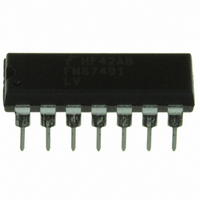
FMS7401LVN14 Fairchild Semiconductor, FMS7401LVN14 Datasheet - Page 30

FMS7401LVN14
Manufacturer Part Number
FMS7401LVN14
Description
IC CTRLR POWER DGTL EEPROM 14DIP
Manufacturer
Fairchild Semiconductor
Datasheet
1.FMS7401LVN.pdf
(81 pages)
Specifications of FMS7401LVN14
Applications
Digital Power Controller
Core Processor
8-Bit
Program Memory Type
EEPROM (1 kB)
Ram Size
64 x 8
Number Of I /o
8
Voltage - Supply
2.7 V ~ 3.6 V
Operating Temperature
-40°C ~ 125°C
Mounting Type
Through Hole
Package / Case
14-DIP (0.300", 7.62mm)
Output Current
5 mA
Input Voltage
2.7 V to 3.6 V
Switching Frequency
2 MHz
Operating Temperature Range
- 40 C to + 125 C
Mounting Style
Through Hole
Lead Free Status / RoHS Status
Lead free / RoHS Compliant
Interface
-
Controller Series
-
Lead Free Status / Rohs Status
Lead free / RoHS Compliant
Other names
FMS7401LVN14_NL
FMS7401LVN14_NL
FMS7401LVN14_NL
FMS7401L
5.3
The Programmable Comparator’s output (C
signal toggles from 0 to 1 when the external input (G4/AIN0 or G2/AIN2) voltage is higher than the programmed voltage
threshold or Uncommitted Amplifier output (A
the programmable digital delay counter to begin incrementing. With each digital delay count, its value is compared against the
value stored in the DD[3:0] bits of the Digital Delay (DDELAY) control register. If C
count equaling DD[3:0] completes, the PWMOFF signal transitions from 0 to 1. This rising edge transition of the PWMOFF
signal is then used to either disable the PWM Timer 1 circuit completely or the current PWM cycle forcing the PWM output
signals to their resting (off) state. The PWMOFF output signal may also be programmed as an input of the G6 port MIW
circuit. Interrupts may be triggered if the G6 port MIW circuit is enabled and configured to trigger its microcontroller hardware
interrupt (EDGEI). Refer to the
Bit 7 of the DDELAY register is the Programmable Comparator circuit enable (COMPEN) bit. If COMPEN=0, the Program-
mable Comparator circuit is disabled and the C
enabled and the C
Bit 6 (PWMINT) of the DDELAY register, if set to 1, selects the PWMOFF signal in place of its G6 input to the MIW circuit.
Software must then enable the MIW PWMOFF/G6 circuit by setting the WKEN[6] bit. The WKEDG[6] bit must also be
cleared to select the rising edge transitions on the PWMOFF signal as its WKPND[6] bit trigger. Software may monitor the
WKPND[6] flag or enable the MIW hardware interrupt (EDGEI) to help detect when the PWMOFF signal is triggered.
Bit 5 (EPWM) of the DDELAY register is the digital delay filter and PWMOFF signal enable bit. The EPWM bit is active low
so that on power-up (after a system reset) the digital delay filter circuit is automatically enabled once the Programmable
Comparator circuit is enabled. If the Programmable Comparator and PWM Timer 1 circuits are enabled, since the filter is
defaulted enabled, the PWMOFF signal may disable the PWM Timer 1 upon a comparator transition. If the digital delay filter
and PWMOFF circuit is not needed, software must set the EPWM bit to 1 disabling the filter before enabling the Programma-
ble Comparator to prevent unwanted disables of the PWM Timer 1 circuit or its outputs.
Bit 4 (OFFMODE) of the DDELAY register determines how the PWMOFF signal affects the PWM Timer 1 circuit. If OFF-
MODE=0 and the Timer 1 circuit is configured in an enabled PWM Mode, Timer 1 is automatically disabled forcing the PWM
T1HS1 and T1HS2 output signals to their resting (off) states with the rising edge of the PWMOFF signal. The T1C0 bit of the
T1CNTRL2 register is cleared, reinitializing the 12-bit TMR1 counter to 0x000. Software must re-enable the Timer 1 circuit to
reactivate the PWM output signals. If OFFMODE=1 and Timer 1 is configured in PWM Mode, the T1HS1 and T1HS2 output
signals are forced to their resting (off) state until the current PWM cycle completes. Once the PWM cycle completes, the
PWMOFF signal releases the T1HS1 and T1HS2 output signals and they resume with their normal operation even if the C
signal remains active (1). The next PWMOFF trigger will not occur until the next rising edge of C
Bits 3-0 (DD[3:0]) of the DDELAY register determine how long to delay the trigger of the PWMOFF signal once the rising
edge of C
stored in the DD[3:0] bits. Once the delay counter completes its DD[3:0] count, if C
triggered. The digital delay counters increment at the device reference clock rate (F
30
Digital Delay Filter with PWMOFF Output
OUT
has been detected. Once the digital delay counter is triggered, the delay count is compared against the value
OUT
signal is generated by the comparison of the two inputs.
Multi-input Wakeup Circuit
OUT
OUT
) is fed into the digital delay filter with a programmable delay time. The C
OUT
), depending on the state of VLOOP. The C
signal is low. If COMPEN=1, the Programmable Comparator circuit is
section of the datasheet regarding for configuration details.
RCLK2
OUT
OUT
remains high, the PWMOFF signal is
).
remains high when the digital delay
4
OUT
rising edge transition triggers
OUT
PRODUCT SPECIFICATION
.
REV. 1.0.3 1/24/05
3
OUT
OUT


