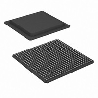
XC3S700AN-4FGG484C Xilinx Inc, XC3S700AN-4FGG484C Datasheet - Page 107

XC3S700AN-4FGG484C
Manufacturer Part Number
XC3S700AN-4FGG484C
Description
IC SPARTAN-3AN FPGA 700K 484FBGA
Manufacturer
Xilinx Inc
Series
Spartan™-3ANr
Datasheets
1.XC3S50A-4VQG100C.pdf
(7 pages)
2.XC3S50AN-4TQG144C.pdf
(2 pages)
3.XC3S50AN-4TQG144C.pdf
(123 pages)
Specifications of XC3S700AN-4FGG484C
Total Ram Bits
368640
Number Of Logic Elements/cells
13248
Number Of Labs/clbs
1472
Number Of I /o
372
Number Of Gates
700000
Voltage - Supply
1.14 V ~ 1.26 V
Mounting Type
Surface Mount
Operating Temperature
0°C ~ 85°C
Package / Case
484-BBGA
No. Of Logic Blocks
13248
No. Of Gates
700000
No. Of Macrocells
13248
Family Type
Spartan-3AN
No. Of Speed Grades
4
No. Of I/o's
372
Lead Free Status / RoHS Status
Lead free / RoHS Compliant
For Use With
122-1528 - KIT STARTER SPARTAN-3 AN
Lead Free Status / RoHS Status
Lead free / RoHS Compliant, Lead free / RoHS Compliant
Other names
122-1556
Available stocks
Company
Part Number
Manufacturer
Quantity
Price
Company:
Part Number:
XC3S700AN-4FGG484C
Manufacturer:
XilinxInc
Quantity:
3 000
Company:
Part Number:
XC3S700AN-4FGG484C
Manufacturer:
Xilinx Inc
Quantity:
10 000
User I/Os by Bank
Table 79
The AWAKE pin is counted as a dual-purpose I/O.
Table 79: User I/Os Per Bank for the XC3S700AN in the FGG484 Package
Table 80: User I/Os Per Bank for the XC3S1400AN in the FGG484 Package
Footprint Migration Differences
Table 81
FPGAs that can affect migration between devices available in the FGG484 package. All other pins unconditionally migrate
between the Spartan-3AN devices available in the FGG484 package.
Spartan-3AN FPGAs are pin compatible with the same density Spartan-3A FPGAs in the FG(G)484 package, although the
Spartan-3A FPGAs require an external configuration source.
In
right. Migration in the other direction is possible depending on how the pin is configured for the device on the right.
Table 81: FGG484 XC3S700AN to XC3S1400AN Footprint Migration/Differences
DS557 (v4.1) April 1, 2011
Product Specification
Top
Right
Bottom
Left
Top
Right
Bottom
Left
Table
FGG484 Ball
Package
Package
Edge
Edge
Total
Total
U16
U7
T8
81, the arrow () indicates that this pin can unconditionally migrate from the device on the left to the device on the
and
summarizes the three footprint and functionality differences between the XC3S700AN and the XC3S1400AN
Table 80
I/O Bank
I/O Bank
0
1
2
3
0
1
2
3
indicate how the user-I/O pins are distributed between the four I/O banks on the FGG484 package.
Number of Differences:
Bank
2
2
2
Maximum I/Os
Maximum I/Os
N.C.
N.C.
N.C.
372
375
92
94
92
94
92
94
95
94
XC3S700AN
195
195
I/O
I/O
58
33
43
61
58
33
43
61
www.xilinx.com
INPUT
INPUT
17
15
11
17
60
17
15
13
17
62
All Possible I/O Pins by Type
All Possible I/O Pins by Type
Spartan-3AN FPGA Family: Pinout Descriptions
Migration
3
DUAL
DUAL
30
21
52
30
21
52
1
0
1
0
INPUT/VREF
INPUT
INPUT
VREF
VREF
33
10
34
XC3S1400AN
8
8
9
8
8
8
8
CLK
CLK
32
32
8
8
8
8
8
8
8
8
107


