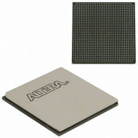
EP2SGX60EF1152I4 Altera, EP2SGX60EF1152I4 Datasheet - Page 296

EP2SGX60EF1152I4
Manufacturer Part Number
EP2SGX60EF1152I4
Description
IC STRATIX II GX 60K 1152-FBGA
Manufacturer
Altera
Series
Stratix® II GXr
Datasheet
1.EP2SGX30DF780C5.pdf
(316 pages)
Specifications of EP2SGX60EF1152I4
Number Of Logic Elements/cells
60440
Number Of Labs/clbs
3022
Total Ram Bits
2544192
Number Of I /o
534
Voltage - Supply
1.15 V ~ 1.25 V
Mounting Type
Surface Mount
Operating Temperature
-40°C ~ 100°C
Package / Case
1152-FBGA
Family Name
Stratix II GX
Number Of Logic Blocks/elements
60440
# I/os (max)
534
Frequency (max)
732.1MHz
Process Technology
SRAM
Operating Supply Voltage (typ)
1.2V
Logic Cells
60440
Ram Bits
2544192
Operating Supply Voltage (min)
1.15V
Operating Supply Voltage (max)
1.25V
Operating Temp Range
-40C to 100C
Operating Temperature Classification
Industrial
Mounting
Surface Mount
Pin Count
1152
Package Type
FC-FBGA
Lead Free Status / RoHS Status
Contains lead / RoHS non-compliant
Number Of Gates
-
Lead Free Status / Rohs Status
Not Compliant
Other names
544-2186
Available stocks
Company
Part Number
Manufacturer
Quantity
Price
Company:
Part Number:
EP2SGX60EF1152I4N
Manufacturer:
ALTERA
Quantity:
534
- Current page: 296 of 316
- Download datasheet (2Mb)
High-Speed I/O
Specifications
t
f
J
W
t
t
Timing unit interval (TUI)
f
f
f
Channel-to-channel skew (TCCS)
Sampling window (SW)
Input jitter
Output jitter
t
t
C
H S C L K
R I S E
F A L L
IN
H S D R
H S D R D P A
DUTY
L O C K
High-Speed Timing Specifications
Table 4–106. High-Speed Timing Specifications and Definitions
Table 4–106
1.2-V HSTL
LVPECL
Column DDIO Output I/O
Table 4–105. Maximum DCD for DDIO Output on Column I/O Pins With PLL in
the Clock Path (Part 2 of 2)
Maximum DCD (ps) for
High-speed receiver/transmitter input and output clock period.
High-speed receiver/transmitter input and output clock frequency.
Deserialization factor (width of parallel data bus).
PLL multiplication factor.
Low-to-high transmission time.
High-to-low transmission time.
The timing budget allowed for skew, propagation delays, and data
sampling window. (TUI = 1/(Receiver Input Clock Frequency ×
Multiplication Factor) = t
Fast PLL input clock frequency
Maximum/minimum LVDS data transfer rate (f
Maximum/minimum LVDS data transfer rate (f
The timing difference between the fastest and the slowest output edges
including t
same fast PLL. The clock is included in the TCCS measurement.
The period of time during which the data must be valid in order to capture
it correctly. The setup and hold times determine the ideal strobe position
within the sampling window.
Peak-to-peak input jitter on high-speed PLLs.
Peak-to-peak output jitter on high-speed PLLs.
Duty cycle on high-speed transmitter output clock.
Lock time for high-speed transmitter and receiver PLLs.
Standard
provides high-speed timing specifications definitions.
CO
variation and clock skew across channels driven by the
Stratix II GX Devices (PLL Output Feeding
C
/w).
-3 Device
155
180
Definitions
DDIO)
-4 and -5 Device
H S D R
H S D R D PA
= 1/TUI), non-DPA.
155
180
= 1/TUI), DPA.
Unit
ps
ps
Related parts for EP2SGX60EF1152I4
Image
Part Number
Description
Manufacturer
Datasheet
Request
R

Part Number:
Description:
4. Serial Configuration Devices Epcs1, Epcs4, Epcs16, Epcs64, And Epcs128 Data Sheet
Manufacturer:
Altera Corporation
Datasheet:

Part Number:
Description:
CYCLONE II STARTER KIT EP2C20N
Manufacturer:
Altera
Datasheet:

Part Number:
Description:
CPLD, EP610 Family, ECMOS Process, 300 Gates, 16 Macro Cells, 16 Reg., 16 User I/Os, 5V Supply, 35 Speed Grade, 24DIP
Manufacturer:
Altera Corporation
Datasheet:

Part Number:
Description:
CPLD, EP610 Family, ECMOS Process, 300 Gates, 16 Macro Cells, 16 Reg., 16 User I/Os, 5V Supply, 15 Speed Grade, 24DIP
Manufacturer:
Altera Corporation
Datasheet:

Part Number:
Description:
Manufacturer:
Altera Corporation
Datasheet:

Part Number:
Description:
CPLD, EP610 Family, ECMOS Process, 300 Gates, 16 Macro Cells, 16 Reg., 16 User I/Os, 5V Supply, 30 Speed Grade, 24DIP
Manufacturer:
Altera Corporation
Datasheet:

Part Number:
Description:
High-performance, low-power erasable programmable logic devices with 8 macrocells, 10ns
Manufacturer:
Altera Corporation
Datasheet:

Part Number:
Description:
High-performance, low-power erasable programmable logic devices with 8 macrocells, 7ns
Manufacturer:
Altera Corporation
Datasheet:

Part Number:
Description:
Classic EPLD
Manufacturer:
Altera Corporation
Datasheet:

Part Number:
Description:
High-performance, low-power erasable programmable logic devices with 8 macrocells, 10ns
Manufacturer:
Altera Corporation
Datasheet:

Part Number:
Description:
Manufacturer:
Altera Corporation
Datasheet:

Part Number:
Description:
Manufacturer:
Altera Corporation
Datasheet:

Part Number:
Description:
Manufacturer:
Altera Corporation
Datasheet:


