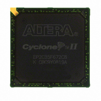
EP2C35F672C8 Altera, EP2C35F672C8 Datasheet - Page 79

EP2C35F672C8
Manufacturer Part Number
EP2C35F672C8
Description
IC CYCLONE II FPGA 33K 672-FBGA
Manufacturer
Altera
Series
Cyclone® IIr
Datasheet
1.EP2C5T144C8N.pdf
(168 pages)
Specifications of EP2C35F672C8
Number Of Logic Elements/cells
33216
Number Of Labs/clbs
2076
Total Ram Bits
483840
Number Of I /o
475
Voltage - Supply
1.15 V ~ 1.25 V
Mounting Type
Surface Mount
Operating Temperature
0°C ~ 85°C
Package / Case
672-FBGA
Family Name
Cyclone® II
Number Of Logic Blocks/elements
33216
# I/os (max)
475
Frequency (max)
402.58MHz
Process Technology
90nm
Operating Supply Voltage (typ)
1.2V
Logic Cells
33216
Ram Bits
483840
Operating Supply Voltage (min)
1.15V
Operating Supply Voltage (max)
1.25V
Operating Temp Range
0C to 85C
Operating Temperature Classification
Commercial
Mounting
Surface Mount
Pin Count
672
Package Type
FBGA
For Use With
NANO-CYCLONE - KIT NANOBOARD AND CYCLONEII DC807-1002 - DAUGHTER CARD ALTERA CYCLONE IIP0301 - DE2 CALL FOR ACADEMIC PRICING544-1733 - PCI KIT W/CYCLONE II EP2C35N
Lead Free Status / RoHS Status
Contains lead / RoHS non-compliant
Number Of Gates
-
Lead Free Status / Rohs Status
Not Compliant
Other names
544-1089
EP2C35F672C8ES
EP2C35F672C8ES
Available stocks
Company
Part Number
Manufacturer
Quantity
Price
Part Number:
EP2C35F672C8
Manufacturer:
ALTERA
Quantity:
20 000
Company:
Part Number:
EP2C35F672C8N
Manufacturer:
YAGEO
Quantity:
500 000
Company:
Part Number:
EP2C35F672C8N
Manufacturer:
ALTERA
Quantity:
500
Part Number:
EP2C35F672C8N
Manufacturer:
ALTERA/阿尔特拉
Quantity:
20 000
SignalTap II
Embedded Logic
Analyzer
Configuration
Operating
Modes
Altera Corporation
February 2007
f
Cyclone II devices support the SignalTap II embedded logic analyzer,
which monitors design operation over a period of time through the IEEE
Std. 1149.1 (JTAG) circuitry. You can analyze internal logic at speed
without bringing internal signals to the I/O pins. This feature is
particularly important for advanced packages, such as FineLine BGA
packages, because it can be difficult to add a connection to a pin during
the debugging process after a board is designed and manufactured.
For more information on the SignalTap II, see the Signal Tap chapter of
the Quartus II Handbook, Volume 3.
The logic, circuitry, and interconnects in the Cyclone II architecture are
configured with CMOS SRAM elements. Altera FPGA devices are
reconfigurable and every device is tested with a high coverage
production test program so you do not have to perform fault testing and
can instead focus on simulation and design verification.
Cyclone II devices are configured at system power-up with data stored in
an Altera configuration device or provided by a system controller. The
Cyclone II device’s optimized interface allows the device to act as
controller in an active serial configuration scheme with EPCS serial
configuration devices. The serial configuration device can be
programmed via SRunner, the ByteBlaster II or USB Blaster download
cable, the Altera Programming Unit (APU), or third-party programmers.
In addition to EPCS serial configuration devices, Altera offers in-system
programmability (ISP)-capable configuration devices that can configure
Cyclone II devices via a serial data stream using the Passive serial (PS)
configuration mode. The PS interface also enables microprocessors to
treat Cyclone II devices as memory and configure them by writing to a
virtual memory location, simplifying reconfiguration. After a Cyclone II
device has been configured, it can be reconfigured in-circuit by resetting
the device and loading new configuration data. Real-time changes can be
made during system operation, enabling innovative reconfigurable
applications.
The Cyclone II architecture uses SRAM configuration elements that
require configuration data to be loaded each time the circuit powers up.
The process of physically loading the SRAM data into the device is called
configuration. During initialization, which occurs immediately after
configuration, the device resets registers, enables I/O pins, and begins to
operate as a logic device. You can use the 10MHz internal oscillator or the
optional CLKUSR pin during the initialization. The 10 MHz internal
oscillator is disabled in user mode. Together, the configuration and
initialization processes are called command mode. Normal device
operation is called user mode.
Cyclone II Device Handbook, Volume 1
Configuration & Testing
®
3–5


