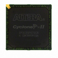
EP2C35F672C8 Altera, EP2C35F672C8 Datasheet - Page 5

EP2C35F672C8
Manufacturer Part Number
EP2C35F672C8
Description
IC CYCLONE II FPGA 33K 672-FBGA
Manufacturer
Altera
Series
Cyclone® IIr
Datasheet
1.EP2C5T144C8N.pdf
(168 pages)
Specifications of EP2C35F672C8
Number Of Logic Elements/cells
33216
Number Of Labs/clbs
2076
Total Ram Bits
483840
Number Of I /o
475
Voltage - Supply
1.15 V ~ 1.25 V
Mounting Type
Surface Mount
Operating Temperature
0°C ~ 85°C
Package / Case
672-FBGA
Family Name
Cyclone® II
Number Of Logic Blocks/elements
33216
# I/os (max)
475
Frequency (max)
402.58MHz
Process Technology
90nm
Operating Supply Voltage (typ)
1.2V
Logic Cells
33216
Ram Bits
483840
Operating Supply Voltage (min)
1.15V
Operating Supply Voltage (max)
1.25V
Operating Temp Range
0C to 85C
Operating Temperature Classification
Commercial
Mounting
Surface Mount
Pin Count
672
Package Type
FBGA
For Use With
NANO-CYCLONE - KIT NANOBOARD AND CYCLONEII DC807-1002 - DAUGHTER CARD ALTERA CYCLONE IIP0301 - DE2 CALL FOR ACADEMIC PRICING544-1733 - PCI KIT W/CYCLONE II EP2C35N
Lead Free Status / RoHS Status
Contains lead / RoHS non-compliant
Number Of Gates
-
Lead Free Status / Rohs Status
Not Compliant
Other names
544-1089
EP2C35F672C8ES
EP2C35F672C8ES
Available stocks
Company
Part Number
Manufacturer
Quantity
Price
Part Number:
EP2C35F672C8
Manufacturer:
ALTERA
Quantity:
20 000
Company:
Part Number:
EP2C35F672C8N
Manufacturer:
YAGEO
Quantity:
500 000
Company:
Part Number:
EP2C35F672C8N
Manufacturer:
ALTERA
Quantity:
500
Part Number:
EP2C35F672C8N
Manufacturer:
ALTERA/阿尔特拉
Quantity:
20 000
Altera Corporation
February 2008
■
■
■
●
●
●
●
●
●
●
●
●
●
●
●
Flexible clock management circuitry
●
●
●
Device configuration
●
●
●
●
●
Intellectual property
●
133-MHz PCI-X 1.0 specification compatibility
High-speed external memory support, including DDR, DDR2,
and SDR SDRAM, and QDRII SRAM supported by drop in
Altera IP MegaCore functions for ease of use
Three dedicated registers per I/O element (IOE): one input
register, one output register, and one output-enable register
Programmable bus-hold feature
Programmable output drive strength feature
Programmable delays from the pin to the IOE or logic array
I/O bank grouping for unique VCCIO and/or VREF bank
settings
MultiVolt
3.3-interfaces
Hot-socketing operation support
Tri-state with weak pull-up on I/O pins before and during
configuration
Programmable open-drain outputs
Series on-chip termination support
Hierarchical clock network for up to 402.5-MHz performance
Up to four PLLs per device provide clock multiplication and
division, phase shifting, programmable duty cycle, and external
clock outputs, allowing system-level clock management and
skew control
Up to 16 global clock lines in the global clock network that drive
throughout the entire device
Fast serial configuration allows configuration times less than
100 ms
Decompression feature allows for smaller programming file
storage and faster configuration times
Supports multiple configuration modes: active serial, passive
serial, and JTAG-based configuration
Supports configuration through low-cost serial configuration
devices
Device configuration supports multiple voltages (either 3.3, 2.5,
or 1.8 V)
Altera megafunction and Altera MegaCore function support,
and Altera Megafunctions Partners Program (AMPP
megafunction support, for a wide range of embedded
processors, on-chip and off-chip interfaces, peripheral
functions, DSP functions, and communications functions and
™
I/O standard support for 1.5-, 1.8-, 2.5-, and
Cyclone II Device Handbook, Volume 1
Introduction
SM
)
1–3


