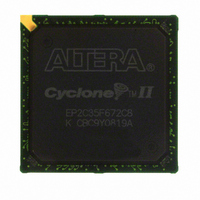
EP2C35F672C8 Altera, EP2C35F672C8 Datasheet - Page 147

EP2C35F672C8
Manufacturer Part Number
EP2C35F672C8
Description
IC CYCLONE II FPGA 33K 672-FBGA
Manufacturer
Altera
Series
Cyclone® IIr
Datasheet
1.EP2C5T144C8N.pdf
(168 pages)
Specifications of EP2C35F672C8
Number Of Logic Elements/cells
33216
Number Of Labs/clbs
2076
Total Ram Bits
483840
Number Of I /o
475
Voltage - Supply
1.15 V ~ 1.25 V
Mounting Type
Surface Mount
Operating Temperature
0°C ~ 85°C
Package / Case
672-FBGA
Family Name
Cyclone® II
Number Of Logic Blocks/elements
33216
# I/os (max)
475
Frequency (max)
402.58MHz
Process Technology
90nm
Operating Supply Voltage (typ)
1.2V
Logic Cells
33216
Ram Bits
483840
Operating Supply Voltage (min)
1.15V
Operating Supply Voltage (max)
1.25V
Operating Temp Range
0C to 85C
Operating Temperature Classification
Commercial
Mounting
Surface Mount
Pin Count
672
Package Type
FBGA
For Use With
NANO-CYCLONE - KIT NANOBOARD AND CYCLONEII DC807-1002 - DAUGHTER CARD ALTERA CYCLONE IIP0301 - DE2 CALL FOR ACADEMIC PRICING544-1733 - PCI KIT W/CYCLONE II EP2C35N
Lead Free Status / RoHS Status
Contains lead / RoHS non-compliant
Number Of Gates
-
Lead Free Status / Rohs Status
Not Compliant
Other names
544-1089
EP2C35F672C8ES
EP2C35F672C8ES
Available stocks
Company
Part Number
Manufacturer
Quantity
Price
Part Number:
EP2C35F672C8
Manufacturer:
ALTERA
Quantity:
20 000
Company:
Part Number:
EP2C35F672C8N
Manufacturer:
YAGEO
Quantity:
500 000
Company:
Part Number:
EP2C35F672C8N
Manufacturer:
ALTERA
Quantity:
500
Part Number:
EP2C35F672C8N
Manufacturer:
ALTERA/阿尔特拉
Quantity:
20 000
Figure 5–4. High-Speed I/O Timing Budget
Note to
(1)
Altera Corporation
February 2008
Internal Clock Period
f
(input
clock
frequency)
Device
operation
in Mbps
t
H S C L K
D U T Y
Table 5–48. RSDS Transmitter Timing Specification (Part 1 of 2)
Symbol
The equation for the high-speed I/O timing budget is:
period = TCCS + RSKM + SW + RSKM.
Figure
5–4:
Conditions
×10
×10
×8
×7
×4
×2
×1
×8
×7
×4
×2
×1
—
0.5 × TCCS
Table 5–48
311 Mbps. RSDS is supported for transmitting from Cyclone II devices.
Cyclone II devices cannot receive RSDS data because the devices are
intended for applications where they will be driving display drivers.
Cyclone II devices support a maximum RSDS data rate of 311 Mbps using
DDIO registers. Cyclone II devices support RSDS only in the commercial
temperature range.
Min
100
10
10
10
10
10
10
80
70
40
20
10
45
–6 Speed Grade
Typ
RSKM
—
—
—
—
—
—
—
—
—
—
—
—
—
shows the RSDS timing budget for Cyclone II devices at
Max(1)
155.5
155.5
155.5
155.5
155.5
311
311
311
311
311
311
311
55
Note (1)
Min
100
10
10
10
10
10
10
80
70
40
20
10
45
–7 Speed Grade
DC Characteristics and Timing Specifications
Typ
—
—
—
—
—
—
—
—
—
—
—
—
—
SW
Max(1)
Cyclone II Device Handbook, Volume 1
155.5
155.5
155.5
155.5
155.5
311
311
311
311
311
311
311
55
Min
100
10
10
10
10
10
10
80
70
40
20
10
45
–8 Speed Grade
RSKM
Typ
—
—
—
—
—
—
—
—
—
—
—
—
—
0.5 × TCCS
Max(1)
155.5
155.5
155.5
155.5
155.5
311
311
311
311
311
311
311
55
Mbps
Mbps
Mbps
Mbps
Mbps
Mbps
MHz
MHz
MHz
MHz
MHz
MHz
Unit
%
5–57


