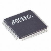
EP1K10TC100-3N Altera, EP1K10TC100-3N Datasheet - Page 59

EP1K10TC100-3N
Manufacturer Part Number
EP1K10TC100-3N
Description
IC ACEX 1K FPGA 10K 100-TQFP
Manufacturer
Altera
Series
ACEX-1K®r
Datasheet
1.EP1K10TC100-3N.pdf
(86 pages)
Specifications of EP1K10TC100-3N
Number Of Logic Elements/cells
576
Number Of Labs/clbs
72
Total Ram Bits
12288
Number Of I /o
66
Number Of Gates
56000
Voltage - Supply
2.375 V ~ 2.625 V
Mounting Type
Surface Mount
Operating Temperature
0°C ~ 85°C
Package / Case
100-TQFP, 100-VQFP
Family Name
ACEX™ 1K
Number Of Usable Gates
10000
Number Of Logic Blocks/elements
576
# I/os (max)
66
Frequency (max)
200MHz
Process Technology
CMOS
Operating Supply Voltage (typ)
2.5V
Logic Cells
576
Ram Bits
12288
Device System Gates
56000
Operating Supply Voltage (min)
2.375V
Operating Supply Voltage (max)
2.625V
Operating Temp Range
0C to 70C
Operating Temperature Classification
Commercial
Mounting
Surface Mount
Pin Count
100
Package Type
TQFP
Lead Free Status / RoHS Status
Lead free / RoHS Compliant
Other names
544-1828
EP1K10TC100-3N
EP1K10TC100-3N
Available stocks
Company
Part Number
Manufacturer
Quantity
Price
Part Number:
EP1K10TC100-3N
Manufacturer:
ALTERA/阿尔特拉
Quantity:
20 000
Altera Corporation
Notes to tables:
(1)
(2)
(3)
(4)
t
t
t
t
t
t
t
t
t
t
t
t
Table 27. External Reference Timing Parameters
DRR
Table 28. External Timing Parameters
INSU
INH
OUTCO
PCISU
PCIH
PCICO
Table 29. External Bidirectional Timing Parameters
INSUBIDIR
INHBIDIR
OUTCOBIDIR
XZBIDIR
ZXBIDIR
Symbol
Symbol
Symbol
External reference timing parameters are factory-tested, worst-case values specified by Altera. A representative
subset of signal paths is tested to approximate typical device applications.
Contact Altera Applications for test circuit specifications and test conditions.
These timing parameters are sample-tested only.
This parameter is measured with the measurement and test conditions, including load, specified in the PCI Local
Bus Specification, Revision 2.2.
Register-to-register delay via four LEs, three row interconnects, and four local
interconnects
Setup time with global clock at IOE register
Hold time with global clock at IOE register
Clock-to-output delay with global clock at IOE register
Setup time with global clock for registers used in PCI designs
Hold time with global clock for registers used in PCI designs
Clock-to-output delay with global clock for registers used in PCI designs
Setup time for bidirectional pins with global clock at same-row or same-
column LE register
Hold time for bidirectional pins with global clock at same-row or same-column
LE register
Clock-to-output delay for bidirectional pins with global clock at IOE register
Synchronous IOE output buffer disable delay
Synchronous IOE output buffer enable delay, slow slew rate = off
Tables 27
and their symbols.
through
Parameter
Parameter
Parameter
29
ACEX 1K Programmable Logic Device Family Data Sheet
describe the ACEX 1K external timing parameters
Note (1)
Note (3)
(2)
(3)
(3)
(3)
(3),
(3),
(3),
CI = 35 pF
CI = 35 pF
CI = 35 pF
Conditions
Conditions
Conditions
(4)
(4)
(4)
59
13


