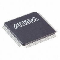
EP1K10TC100-3N Altera, EP1K10TC100-3N Datasheet - Page 58

EP1K10TC100-3N
Manufacturer Part Number
EP1K10TC100-3N
Description
IC ACEX 1K FPGA 10K 100-TQFP
Manufacturer
Altera
Series
ACEX-1K®r
Datasheet
1.EP1K10TC100-3N.pdf
(86 pages)
Specifications of EP1K10TC100-3N
Number Of Logic Elements/cells
576
Number Of Labs/clbs
72
Total Ram Bits
12288
Number Of I /o
66
Number Of Gates
56000
Voltage - Supply
2.375 V ~ 2.625 V
Mounting Type
Surface Mount
Operating Temperature
0°C ~ 85°C
Package / Case
100-TQFP, 100-VQFP
Family Name
ACEX™ 1K
Number Of Usable Gates
10000
Number Of Logic Blocks/elements
576
# I/os (max)
66
Frequency (max)
200MHz
Process Technology
CMOS
Operating Supply Voltage (typ)
2.5V
Logic Cells
576
Ram Bits
12288
Device System Gates
56000
Operating Supply Voltage (min)
2.375V
Operating Supply Voltage (max)
2.625V
Operating Temp Range
0C to 70C
Operating Temperature Classification
Commercial
Mounting
Surface Mount
Pin Count
100
Package Type
TQFP
Lead Free Status / RoHS Status
Lead free / RoHS Compliant
Other names
544-1828
EP1K10TC100-3N
EP1K10TC100-3N
Available stocks
Company
Part Number
Manufacturer
Quantity
Price
Part Number:
EP1K10TC100-3N
Manufacturer:
ALTERA/阿尔特拉
Quantity:
20 000
ACEX 1K Programmable Logic Device Family Data Sheet
Notes to tables:
(1)
(2)
(3)
(4)
(5)
(6)
(7)
58
t
t
t
t
t
t
t
t
t
t
t
t
t
DIN2IOE
DIN2LE
DIN2DATA
DCLK2IOE
DCLK2LE
SAMELAB
SAMEROW
SAMECOLUMN
DIFFROW
TWOROWS
LEPERIPH
LABCARRY
LABCASC
Table 26. Interconnect Timing Microparameters
Symbol
Microparameters are timing delays contributed by individual architectural elements. These parameters cannot be
measured explicitly.
Operating conditions: V
Operating conditions: V
Operating conditions: V
Because the RAM in the EAB is self-timed, this parameter can be ignored when the WE signal is registered.
EAB macroparameters are internal parameters that can simplify predicting the behavior of an EAB at its boundary;
these parameters are calculated by summing selected microparameters.
These parameters are worst-case values for typical applications. Post-compilation timing simulation and timing
analysis are required to determine actual worst-case performance.
Delay from dedicated input pin to IOE control input
Delay from dedicated input pin to LE or EAB control input
Delay from dedicated input or clock to LE or EAB data
Delay from dedicated clock pin to IOE clock
Delay from dedicated clock pin to LE or EAB clock
Routing delay for an LE driving another LE in the same LAB
Routing delay for a row IOE, LE, or EAB driving a row IOE, LE, or EAB in the
same row
Routing delay for an LE driving an IOE in the same column
Routing delay for a column IOE, LE, or EAB driving an LE or EAB in a different
row
Routing delay for a row IOE or EAB driving an LE or EAB in a different row
Routing delay for an LE driving a control signal of an IOE via the peripheral
control bus
Routing delay for the carry-out signal of an LE driving the carry-in signal of a
different LE in a different LAB
Routing delay for the cascade-out signal of an LE driving the cascade-in
signal of a different LE in a different LAB
CCIO
CCIO
CCIO
= 3.3 V ± 10% for commercial or industrial and extended use in ACEX 1K devices
= 2.5 V ± 5% for commercial or industrial and extended use in ACEX 1K devices.
= 2.5 V or 3.3 V.
Parameter
Note (1)
Altera Corporation
(7)
(7)
(7)
(7)
(7)
(7)
(7)
(7)
(7)
(7)
(7)
Conditions


