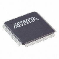
EP1K10TC100-3N Altera, EP1K10TC100-3N Datasheet - Page 4

EP1K10TC100-3N
Manufacturer Part Number
EP1K10TC100-3N
Description
IC ACEX 1K FPGA 10K 100-TQFP
Manufacturer
Altera
Series
ACEX-1K®r
Datasheet
1.EP1K10TC100-3N.pdf
(86 pages)
Specifications of EP1K10TC100-3N
Number Of Logic Elements/cells
576
Number Of Labs/clbs
72
Total Ram Bits
12288
Number Of I /o
66
Number Of Gates
56000
Voltage - Supply
2.375 V ~ 2.625 V
Mounting Type
Surface Mount
Operating Temperature
0°C ~ 85°C
Package / Case
100-TQFP, 100-VQFP
Family Name
ACEX™ 1K
Number Of Usable Gates
10000
Number Of Logic Blocks/elements
576
# I/os (max)
66
Frequency (max)
200MHz
Process Technology
CMOS
Operating Supply Voltage (typ)
2.5V
Logic Cells
576
Ram Bits
12288
Device System Gates
56000
Operating Supply Voltage (min)
2.375V
Operating Supply Voltage (max)
2.625V
Operating Temp Range
0C to 70C
Operating Temperature Classification
Commercial
Mounting
Surface Mount
Pin Count
100
Package Type
TQFP
Lead Free Status / RoHS Status
Lead free / RoHS Compliant
Other names
544-1828
EP1K10TC100-3N
EP1K10TC100-3N
Available stocks
Company
Part Number
Manufacturer
Quantity
Price
Part Number:
EP1K10TC100-3N
Manufacturer:
ALTERA/阿尔特拉
Quantity:
20 000
ACEX 1K Programmable Logic Device Family Data Sheet
General
Description
Notes:
(1)
(2)
4
16-bit loadable counter
16-bit accumulator
16-to-1 multiplexer
16-bit multiplier with 3-stage
256
256
Table 4. ACEX 1K Device Performance
This application uses combinatorial inputs and outputs.
This application uses registered inputs and outputs.
16 RAM read cycle speed
16 RAM write cycle speed
Application
(1)
pipeline(2)
Altera
combining look-up table (LUT) architecture with EABs. LUT-based logic
provides optimized performance and efficiency for data-path, register
intensive, mathematical, or digital signal processing (DSP) designs, while
EABs implement RAM, ROM, dual-port RAM, or first-in first-out (FIFO)
functions. These elements make ACEX 1K suitable for complex logic
functions and memory functions such as digital signal processing, wide
data-path manipulation, data transformation and microcontrollers, as
required in high-performance communications applications. Based on
reconfigurable CMOS SRAM elements, the ACEX 1K architecture
incorporates all features necessary to implement common gate array
megafunctions, along with a high pin count to enable an effective interface
with system components. The advanced process and the low voltage
requirement of the 2.5-V core allow ACEX 1K devices to meet the
requirements of low-cost, high-volume applications ranging from DSL
modems to low-cost switches.
The ability to reconfigure ACEX 1K devices enables complete testing prior
to shipment and allows the designer to focus on simulation and design
verification. ACEX 1K device reconfigurability eliminates inventory
management for gate array designs and test vector generation for fault
coverage.
Table 4
All performance results were obtained with Synopsys DesignWare or
LPM functions. Special design techniques are not required to implement
the applications; the designer simply infers or instantiates a function in a
Verilog HDL, VHDL, Altera Hardware Description Language (AHDL), or
schematic design file.
(2)
(2)
®
shows ACEX 1K device performance for some common designs.
ACEX 1K devices provide a die-efficient, low-cost architecture by
592
LEs
Resources
16
16
10
0
0
Used
EABs
0
0
0
0
1
1
285
285
156
278
185
3.5
-1
Speed Grade
Performance
232
232
131
196
143
4.5
-2
Altera Corporation
185
185
143
111
6.6
93
-3
Units
MHz
MHz
MHz
MHz
MHz
ns


