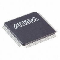
EP1K10TC100-3N Altera, EP1K10TC100-3N Datasheet - Page 36

EP1K10TC100-3N
Manufacturer Part Number
EP1K10TC100-3N
Description
IC ACEX 1K FPGA 10K 100-TQFP
Manufacturer
Altera
Series
ACEX-1K®r
Datasheet
1.EP1K10TC100-3N.pdf
(86 pages)
Specifications of EP1K10TC100-3N
Number Of Logic Elements/cells
576
Number Of Labs/clbs
72
Total Ram Bits
12288
Number Of I /o
66
Number Of Gates
56000
Voltage - Supply
2.375 V ~ 2.625 V
Mounting Type
Surface Mount
Operating Temperature
0°C ~ 85°C
Package / Case
100-TQFP, 100-VQFP
Family Name
ACEX™ 1K
Number Of Usable Gates
10000
Number Of Logic Blocks/elements
576
# I/os (max)
66
Frequency (max)
200MHz
Process Technology
CMOS
Operating Supply Voltage (typ)
2.5V
Logic Cells
576
Ram Bits
12288
Device System Gates
56000
Operating Supply Voltage (min)
2.375V
Operating Supply Voltage (max)
2.625V
Operating Temp Range
0C to 70C
Operating Temperature Classification
Commercial
Mounting
Surface Mount
Pin Count
100
Package Type
TQFP
Lead Free Status / RoHS Status
Lead free / RoHS Compliant
Other names
544-1828
EP1K10TC100-3N
EP1K10TC100-3N
Available stocks
Company
Part Number
Manufacturer
Quantity
Price
Part Number:
EP1K10TC100-3N
Manufacturer:
ALTERA/阿尔特拉
Quantity:
20 000
ACEX 1K Programmable Logic Device Family Data Sheet
ClockLock &
ClockBoost
Features
36
f
For more information, search for “SameFrame” in MAX+PLUS II Help.
Note:
(1)
To support high-speed designs, -1 and -2 speed grade ACEX 1K devices
offer ClockLock and ClockBoost circuitry containing a phase-locked loop
(PLL) that is used to increase design speed and reduce resource usage. The
ClockLock circuitry uses a synchronizing PLL that reduces the clock delay
and skew within a device. This reduction minimizes clock-to-output and
setup times while maintaining zero hold times. The ClockBoost circuitry,
which provides a clock multiplier, allows the designer to enhance device
area efficiency by sharing resources within the device. The ClockBoost
feature allows the designer to distribute a low-speed clock and multiply
that clock on-device. Combined, the ClockLock and ClockBoost features
provide significant improvements in system performance and
bandwidth.
The ClockLock and ClockBoost features in ACEX 1K devices are enabled
through the Altera software. External devices are not required to use these
features. The output of the ClockLock and ClockBoost circuits is not
available at any of the device pins.
The ClockLock and ClockBoost circuitry lock onto the rising edge of the
incoming clock. The circuit output can drive the clock inputs of registers
only; the generated clock cannot be gated or inverted.
The dedicated clock pin (GCLK1) supplies the clock to the ClockLock and
ClockBoost circuitry. When the dedicated clock pin is driving the
ClockLock or ClockBoost circuitry, it cannot drive elsewhere in the device.
EP1K10
EP1K30
EP1K50
EP1K100
Table 10. ACEX 1K SameFrame Pin-Out Support
This option is supported with a 256-pin FineLine BGA package and SameFrame
migration.
Device
FineLine
256-Pin
BGA
v
v
v
v
FineLine
Altera Corporation
484-Pin
BGA
v
v
(1)
(1)


