DSPB56371AF150 Freescale Semiconductor, DSPB56371AF150 Datasheet - Page 8
DSPB56371AF150
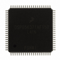
Manufacturer Part Number
DSPB56371AF150
Description
IC DSP 24BIT 150MHZ 80-LQFP
Manufacturer
Freescale Semiconductor
Series
Symphony™r
Type
Audio Processorr
Datasheet
1.DSPB56371AF180.pdf
(68 pages)
Specifications of DSPB56371AF150
Interface
Host Interface, I²C, SAI, SPI
Clock Rate
150MHz
Non-volatile Memory
ROM (384 kB)
On-chip Ram
264kB
Voltage - I/o
3.30V
Voltage - Core
1.25V
Operating Temperature
-40°C ~ 115°C
Mounting Type
Surface Mount
Package / Case
80-LQFP
Product
DSPs
Data Bus Width
24 bit
Processor Series
DSP563xx
Core
56000
Numeric And Arithmetic Format
Fixed-Point
Device Million Instructions Per Second
150 MIPs
Maximum Clock Frequency
150 MHz
Program Memory Size
192 KB
Data Ram Size
264 KB
Operating Supply Voltage
1.25 V, 3.3 V
Maximum Operating Temperature
+ 115 C
Mounting Style
SMD/SMT
Minimum Operating Temperature
- 40 C
Lead Free Status / RoHS Status
Lead free / RoHS Compliant
Available stocks
Company
Part Number
Manufacturer
Quantity
Price
Company:

Part Number:
DSPB56371AF150
Manufacturer:
Freescale Semiconductor
Quantity:
10 000
Part Number:
DSPB56371AF150
Manufacturer:
FREESCALE
Quantity:
20 000


DSP56371 Overview
2.4.6
The clock generator in the DSP56300 core is composed of two main blocks: the PLL, which performs
clock input division, frequency multiplication, skew elimination and the clock generator (CLKGEN),
which performs low-power division and clock pulse generation. PLL-based clocking:
The PLL allows the processor to operate at a high internal clock frequency using a low frequency clock
input. This feature offers two immediate benefits:
2.4.7
The memory space of the DSP56300 core is partitioned into program memory space, X data memory space
and Y data memory space. The data memory space is divided into X and Y data memory in order to work
with the two Address ALUs and to feed two operands simultaneously to the Data ALU. Memory space
includes internal RAM and ROM and can not be expanded off-chip.
There is an instruction patch module. The patch module is used to patch program ROM. The memory
switch mode is used to increase the size of program RAM as needed (switch from X data RAM and/or Y
data RAM).
There are on-chip ROMs for program and bootstrap memory (64K x 24-bit), X ROM (32K x 24-bit) and
Y ROM (32K x 24-bit).
More information on the internal memory is provided in the
2.4.8
Memory cannot be expanded off-chip. There is no external memory bus.
8
•
•
•
•
•
•
Triggering from interrupt lines and all peripherals
Allows change of low-power divide factor (DF) without loss of lock
Provides output clock with skew elimination
Provides a wide range of frequency multiplications (1 to 255), predivider factors (1 to 31), PLL
feedback multiplier (2 or 4), output divide factor (1, 2 or 4), and a power-saving clock divider
(2
A lower frequency clock input reduces the overall electromagnetic interference generated by a
system.
The ability to oscillate at different frequencies reduces costs by eliminating the need to add
additional oscillators to a system.
The PLL will momentarily overshoot the target frequency when the PLL is first enabled or
when the VCO frequency is modified. It is important that when modifying the PLL
frequency or enabling the PLL that the two-step procedure defined in
Overview
i
: i = 0 to 7) to reduce clock noise
PLL-based Clock Oscillator
On-Chip Memory
Off-Chip Memory Expansion
be followed.
DSP56371 Data Sheet, Rev. 4.1
NOTE
DSP56371 User’s Manual, Memory
Section 3, DSP56371
Freescale Semiconductor
section.
Related parts for DSPB56371AF150
Image
Part Number
Description
Manufacturer
Datasheet
Request
R

Part Number:
Description:
Manufacturer:
Freescale Semiconductor, Inc
Datasheet:
Part Number:
Description:
Manufacturer:
Freescale Semiconductor, Inc
Datasheet:
Part Number:
Description:
Manufacturer:
Freescale Semiconductor, Inc
Datasheet:
Part Number:
Description:
Manufacturer:
Freescale Semiconductor, Inc
Datasheet:
Part Number:
Description:
Manufacturer:
Freescale Semiconductor, Inc
Datasheet:
Part Number:
Description:
Manufacturer:
Freescale Semiconductor, Inc
Datasheet:
Part Number:
Description:
Manufacturer:
Freescale Semiconductor, Inc
Datasheet:
Part Number:
Description:
Manufacturer:
Freescale Semiconductor, Inc
Datasheet:
Part Number:
Description:
Manufacturer:
Freescale Semiconductor, Inc
Datasheet:
Part Number:
Description:
Manufacturer:
Freescale Semiconductor, Inc
Datasheet:
Part Number:
Description:
Manufacturer:
Freescale Semiconductor, Inc
Datasheet:
Part Number:
Description:
Manufacturer:
Freescale Semiconductor, Inc
Datasheet:
Part Number:
Description:
Manufacturer:
Freescale Semiconductor, Inc
Datasheet:
Part Number:
Description:
Manufacturer:
Freescale Semiconductor, Inc
Datasheet:
Part Number:
Description:
Manufacturer:
Freescale Semiconductor, Inc
Datasheet: