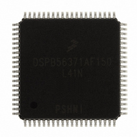
DSPB56371AF150 Freescale Semiconductor, DSPB56371AF150 Datasheet - Page 14

DSPB56371AF150
Manufacturer Part Number
DSPB56371AF150
Description
IC DSP 24BIT 150MHZ 80-LQFP
Manufacturer
Freescale Semiconductor
Series
Symphony™r
Type
Audio Processorr
Datasheet
1.DSPB56371AF180.pdf
(68 pages)
Specifications of DSPB56371AF150
Interface
Host Interface, I²C, SAI, SPI
Clock Rate
150MHz
Non-volatile Memory
ROM (384 kB)
On-chip Ram
264kB
Voltage - I/o
3.30V
Voltage - Core
1.25V
Operating Temperature
-40°C ~ 115°C
Mounting Type
Surface Mount
Package / Case
80-LQFP
Product
DSPs
Data Bus Width
24 bit
Processor Series
DSP563xx
Core
56000
Numeric And Arithmetic Format
Fixed-Point
Device Million Instructions Per Second
150 MIPs
Maximum Clock Frequency
150 MHz
Program Memory Size
192 KB
Data Ram Size
264 KB
Operating Supply Voltage
1.25 V, 3.3 V
Maximum Operating Temperature
+ 115 C
Mounting Style
SMD/SMT
Minimum Operating Temperature
- 40 C
Lead Free Status / RoHS Status
Lead free / RoHS Compliant
Available stocks
Company
Part Number
Manufacturer
Quantity
Price
Company:
Part Number:
DSPB56371AF150
Manufacturer:
Freescale Semiconductor
Quantity:
10 000
Part Number:
DSPB56371AF150
Manufacturer:
FREESCALE
Quantity:
20 000
Signal/Connection Descriptions
3.3
3.4
3.5
14
CORE_GND (4) Core Ground—The Core ground should be provided with an extremely low-impedance path to
PINIT/NMI
Ground Name
PLLD_GND(1) PLL Ground—The PLL ground should be provided with an extremely low-impedance path to
PLLA_GND(1)
PLLP_GND(1)
IO_GND (5)
EXTAL
Signal
Signal
SCAN
Name
Name
Ground
SCAN
Clock and PLL
Type
Input
Type
Input
Input
PLL Ground—The PLL ground should be provided with an extremely low-impedance path to
ground. The user must provide adequate external decoupling capacitors.
ground. The user must provide adequate external decoupling capacitors.
ground. This connection must be tied externally to all other chip ground connections. The user must
provide adequate external decoupling capacitors.
SHI, ESAI, ESAI_1, DAX and Timer I/O Ground—IO_GND is an isolated ground for the SHI, ESAI,
ESAI_1, DAX and Timer I/O. This connection must be tied externally to all other chip ground
connections. The user must provide adequate external decoupling capacitors.
During
during
Reset
Reset
State
State
Input
Input
Input
SCAN—Manufacturing test pin. This pin should be pulled low.
Internal Pull down resistor.
External Clock Input—An external clock source must be connected to EXTAL in
order to supply the clock to the internal clock generator and PLL.
This input is 5 V tolerant.
PLL Initial/Nonmaskable Interrupt—During assertion of RESET, the value of
PINIT/NMI is written into the PLL Enable (PEN) bit of the PLL control register,
determining whether the PLL is enabled or disabled. After RESET de assertion
and during normal instruction processing, the PINIT/NMI Schmitt-trigger input is
a negative-edge-triggered nonmaskable interrupt (NMI) request internally
synchronized to internal system clock.
Internal Pull up resistor.
This input is 5 V tolerant.
Table 5. Clock and PLL Signals
DSP56371 Data Sheet, Rev. 4.1
Table 4. SCAN Signals
Table 3. Grounds
Description
Signal Description
Signal Description
Freescale Semiconductor


