EPM570GF100C5N Altera, EPM570GF100C5N Datasheet - Page 6
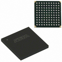
EPM570GF100C5N
Manufacturer Part Number
EPM570GF100C5N
Description
IC MAX II CPLD 570 LE 100-FBGA
Manufacturer
Altera
Series
MAX® IIr
Datasheets
1.EPM240GT100C5N.pdf
(6 pages)
2.EPM240GT100C5N.pdf
(88 pages)
3.EPM240GM100C5N.pdf
(10 pages)
Specifications of EPM570GF100C5N
Programmable Type
In System Programmable
Delay Time Tpd(1) Max
5.4ns
Voltage Supply - Internal
1.71 V ~ 1.89 V
Number Of Logic Elements/blocks
570
Number Of Macrocells
440
Number Of I /o
76
Operating Temperature
0°C ~ 85°C
Mounting Type
Surface Mount
Package / Case
100-FBGA
Voltage
1.8V
Memory Type
FLASH
Number Of Logic Elements/cells
570
Lead Free Status / RoHS Status
Lead free / RoHS Compliant
Features
-
Other names
544-1730
Available stocks
Company
Part Number
Manufacturer
Quantity
Price


MAX II Device Family
6
Preliminary
If the OSCENA port is asserted at the power-up condition in the design, the
OSC output port does not exhibit a high or low pulse, but instead
immediately starts clocking upon entry into user mode. For the asserted
or de-asserted OSCENA power-up possibilities, it is undetermined
whether the OSC output starts with a rising or falling edge. You should
assume an unknown “X” on the OSC output port for all power-up
conditions in your design with EPM1270 ES devices.
1
Schmitt Trigger Slow Falling Input Edge Glitch
The Schmitt trigger input buffer is an optional feature on each I/O pin in
MAX II devices to help maximize noise immunity on input pins. For
EPM1270 ES devices, the 3.3-V or 2.5-V Schmitt trigger input option may
glitch when driven by high-to-low signal transitions with fall times
greater than 1 µs. Low-to-high signal transitions are not susceptible to
glitch and reliably accept signals with rise times up to 200 ms.
The workaround to improve the Schmitt trigger falling edge input
performance beyond 1-µs fall times is to enable the programmable input
delay for that particular pin. Enabling the programmable input delay for
the input pin allows the Schmitt trigger to accept fall times up to 200 ms.
The programmable input delay adds a delay to the input delay path of
~2.1 ns for -4 speed grade and ~2.6 ns for -5 speed grade. This option can
be set in the Assignment Editor (Assignments menu) on a pin-by-pin
basis. The procedure to set this in the Quartus II software for a pin is
shown below:
1.
2.
3.
4.
5.
This procedure turns on the input delay for the selected input pin.
Select input pin name in the design file.
Right-click and select Locate in Assignment Editor.
Double-click the cell under Assignment Name and select Input
Delay from Pin to Internal Cells in the drop-down list.
Double-click the Value cell to the right of the assignment name just
made and enter 1.
Click Save (File menu).
Production devices do not exhibit the high or low pulse after
power-up for the de-asserted OSCENA signal. For these devices,
OSC stays high at power-up and does not clock until enabled
with OSCENA.
Altera Corporation
Related parts for EPM570GF100C5N
Image
Part Number
Description
Manufacturer
Datasheet
Request
R

Part Number:
Description:
MAX II Device Family
Manufacturer:
Altera
Datasheet:

Part Number:
Description:
CYCLONE II STARTER KIT EP2C20N
Manufacturer:
Altera
Datasheet:

Part Number:
Description:
CPLD, EP610 Family, ECMOS Process, 300 Gates, 16 Macro Cells, 16 Reg., 16 User I/Os, 5V Supply, 35 Speed Grade, 24DIP
Manufacturer:
Altera Corporation
Datasheet:
Part Number:
Description:
CPLD, EP610 Family, ECMOS Process, 300 Gates, 16 Macro Cells, 16 Reg., 16 User I/Os, 5V Supply, 15 Speed Grade, 24DIP
Manufacturer:
Altera Corporation
Datasheet:
Part Number:
Description:
Manufacturer:
Altera Corporation
Datasheet:
Part Number:
Description:
CPLD, EP610 Family, ECMOS Process, 300 Gates, 16 Macro Cells, 16 Reg., 16 User I/Os, 5V Supply, 30 Speed Grade, 24DIP
Manufacturer:
Altera Corporation
Datasheet:
Part Number:
Description:
High-performance, low-power erasable programmable logic devices with 8 macrocells, 10ns
Manufacturer:
Altera Corporation
Datasheet:
Part Number:
Description:
High-performance, low-power erasable programmable logic devices with 8 macrocells, 7ns
Manufacturer:
Altera Corporation
Datasheet:
Part Number:
Description:
Classic EPLD
Manufacturer:
Altera Corporation
Datasheet:
Part Number:
Description:
High-performance, low-power erasable programmable logic devices with 8 macrocells, 10ns
Manufacturer:
Altera Corporation
Datasheet:
Part Number:
Description:
Manufacturer:
Altera Corporation
Datasheet:
Part Number:
Description:
Manufacturer:
Altera Corporation
Datasheet:
Part Number:
Description:
Manufacturer:
Altera Corporation
Datasheet: