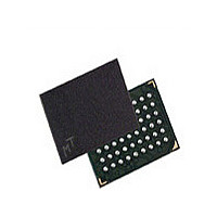
MT48H8M16LFB4-75 IT:J TR Micron Technology Inc, MT48H8M16LFB4-75 IT:J TR Datasheet - Page 33

MT48H8M16LFB4-75 IT:J TR
Manufacturer Part Number
MT48H8M16LFB4-75 IT:J TR
Description
Manufacturer
Micron Technology Inc
Type
Mobile SDRAMr
Datasheet
1.MT48H8M16LFB4-75_ITJ_TR.pdf
(75 pages)
Specifications of MT48H8M16LFB4-75 IT:J TR
Organization
8Mx16
Density
128Mb
Address Bus
14b
Access Time (max)
8/5.4ns
Maximum Clock Rate
133MHz
Operating Supply Voltage (typ)
1.8V
Package Type
VFBGA
Operating Temp Range
-40C to 85C
Operating Supply Voltage (max)
1.95V
Operating Supply Voltage (min)
1.7V
Supply Current
70mA
Pin Count
54
Mounting
Surface Mount
Operating Temperature Classification
Industrial
Lead Free Status / Rohs Status
Compliant
PDF: 09005aef832ff1ea/Source: 09005aef832ff1ac
sdr_mobile_sdram_cmd_op_timing_dia_fr10_08__3.fm - Rev. E 4/09 EN
10. For a READ without auto precharge interrupted by a READ (with or without auto pre-
11. For a READ without auto precharge interrupted by a WRITE (with or without auto pre-
12. For a WRITE without auto precharge interrupted by a READ (with or without auto pre-
13. For a WRITE without auto precharge interrupted by a WRITE (with or without auto pre-
14. For a READ with auto precharge interrupted by a READ (with or without auto precharge),
15. For a READ with auto precharge interrupted by a WRITE (with or without auto precharge),
16. For a WRITE with auto precharge interrupted by a READ (with or without auto precharge),
17. For a WRITE with auto precharge interrupted by a WRITE (with or without auto precharge),
6. All states and sequences not shown are illegal or reserved.
7. READs or WRITEs to bank m listed in the Command/Action column include READs or WRITEs
8. Concurrent auto precharge: Bank n will initiate the auto precharge command when its
9. The burst in bank n continues as initiated.
with auto precharge enabled and READs or WRITEs with auto precharge disabled.
burst has been interrupted by bank m burst.
charge), the READ to bank m will interrupt the READ on bank n, CAS latency (CL) later.
charge), the WRITE to bank m will interrupt the READ on bank n when registered. DQM
should be used one clock prior to the WRITE command to prevent bus contention.
charge), the READ to bank m will interrupt the WRITE on bank n when registered, with the
data-out appearing CL later. The last valid WRITE to bank n will be data-in registered one
clock prior to the READ to bank m.
charge), the WRITE to bank m will interrupt the WRITE on bank n when registered. The last
valid WRITE to bank n will be data-in registered one clock prior to the READ to bank m.
the READ to bank m will interrupt the READ on bank n, CL later. The PRECHARGE to bank n
will begin when the READ to bank m is registered.
the WRITE to bank m will interrupt the READ on bank n when registered. DQM should be
used two clocks prior to the WRITE command to prevent bus contention. The PRECHARGE
to bank n will begin when the WRITE to bank m is registered.
the READ to bank m will interrupt the WRITE on bank n when registered, with the data-out
appearing CL later. The PRECHARGE to bank n will begin after
begins when the READ to bank m is registered. The last valid WRITE bank n will be data-in
registered one clock prior to the READ to bank m.
the WRITE to bank m will interrupt the WRITE on bank n when registered. The PRECHARGE
to bank n will begin after
istered. The last valid WRITE to bank n will be data registered one clock to the WRITE to
bank m.
128Mb: 8 Meg x 16, 4 Meg x 32 Mobile SDRAM
t
WR is met, where
33
Micron Technology, Inc., reserves the right to change products or specifications without notice.
t
WR begins when the WRITE to bank m is reg-
t
WR is met, where
©2008 Micron Technology, Inc. All rights reserved.
Operations
t
WR


