AD7244JRZ Analog Devices Inc, AD7244JRZ Datasheet
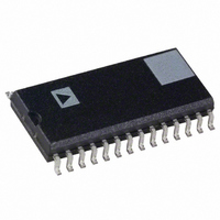
IC DAC 14BIT LC2MOS DUAL 28SOIC

AD7244JRZ

Manufacturer Part Number
AD7244JRZ
Description
IC DAC 14BIT LC2MOS DUAL 28SOIC
Manufacturer
Analog Devices Inc
Datasheet

Specifications of AD7244JRZ

Data Interface
Serial
Settling Time
4µs
Number Of Bits
14
Number Of Converters
2
Voltage Supply Source
Dual ±
Power Dissipation (max)
205mW
Operating Temperature
-40°C ~ 85°C
Mounting Type
Surface Mount
Package / Case
28-SOIC (7.5mm Width)
Resolution (bits)
14bit
Sampling Rate
250kSPS
Input Channel Type
Serial
Supply Current
27mA
Digital Ic Case Style
SOIC
No. Of Pins
28
Supply Voltage Range - Analog
± 4.75V To ± 5.25V
Rohs Compliant
Yes
Lead Free Status / RoHS Status
Lead free / RoHS Compliant

Available stocks

Company
Part Number
Manufacturer
Quantity
Price
Part Number:
AD7244JRZ
Manufacturer:
Analog Devices Inc
Quantity:
135
Part Number:
AD7244JRZ
Manufacturer:
ADI/亚德诺
Quantity:
20 000
a
GENERAL DESCRIPTION
The AD7242/AD7244 is a fast, complete, dual 12-bit/14-bit
voltage output D/A converter. It consists of a 12-bit/14-bit
DAC, 3 V buried Zener reference, DAC output amplifiers and
high speed serial interface logic.
Interfacing to both DACs is serial, minimizing pin count and
allowing a small package size. Standard control signals allow
interfacing to most DSP processors and microcontrollers.
Asynchronous control of DAC updating for both DACs is made
possible with a separate LDAC input for each DAC.
The AD7242/AD7244 operates from 5 V power supplies,
providing an analog output range of 3 V. A REF OUT/REF
IN function allows the DACs to be driven from the on-chip 3 V
reference or from an external reference source.
The AD7242/AD7244 is fabricated in Linear Compatible
CMOS (LC
combines precision bipolar circuits with low power CMOS
logic. Both parts are available in a 24-pin, 0.3-inch wide, plastic
or hermetic dual-in-line package (DIP) and in a 28-pin, plastic
small outline (SOIC) package. The AD7242 and AD7244 are
available in the same pinout to allow easy upgrade from 12-bit
to 14-bit performance.
REV. A
Information furnished by Analog Devices is believed to be accurate and
reliable. However, no responsibility is assumed by Analog Devices for its
use, nor for any infringements of patents or other rights of third parties
which may result from its use. No license is granted by implication or
otherwise under any patent or patent rights of Analog Devices.
FEATURES
Two 12-Bit/14-Bit DACs with Output Amplifiers
On-Chip Voltage Reference
Fast Settling Time
High Speed Serial Interface
Operates from
Specified Over –40 C to +85 C in Plastic Packages
Low Power – 130 mW typ
AD7242: 12-Bit Resolution
AD7244: 14-Bit Resolution
AD7242: 3 s to
AD7244: 4 s to
2
MOS), an advanced mixed technology process that
5 V Supplies
1/2 LSB
1/2 LSB
PRODUCT HIGHLIGHTS
1. Complete, Dual 12-Bit/14-Bit DACs
2. High Speed Serial Interface
3. Small Package Size
One Technology Way, P.O. Box 9106, Norwood, MA 02062-9106, U.S.A.
Tel: 617/329-4700
Fax: 617/326-8703
The AD7242/AD7244 provides the complete function for
generating voltages to 12-bit/14-bit resolution. The part
features an on-chip reference, output buffer amplifiers and
two 12-bit/14-bit D/A converters.
The AD7242/AD7244 provides a high speed, easy-to-use,
serial interface allowing direct interfacing to DSP processors
and microcontrollers. A separate serial port is provided for
each DAC.
The AD7242/AD7244 is available in a 24-pin DIP and a 28-
pin SOIC package offering considerable space saving over
comparable solutions.
12-Bit/14-Bit Serial DACs
FUNCTIONAL BLOCK DIAGRAM
LC
2
World Wide Web Site: http://www.analog.com
MOS Dual, Complete,
AD7242/AD7244
© Analog Devices, Inc., 1996

Related parts for AD7244JRZ

AD7244JRZ Summary of contents

Page 1

FEATURES Two 12-Bit/14-Bit DACs with Output Amplifiers AD7242: 12-Bit Resolution AD7244: 14-Bit Resolution On-Chip Voltage Reference Fast Settling Time AD7242 1/2 LSB AD7244 1/2 LSB High Speed Serial Interface Operates from 5 V ...

Page 2

AD7242/AD7244–SPECIFICATIONS All Specifications unless otherwise noted.) MIN MAX Parameter J, A Versions DC ACCURACY Resolution 12 Integral Nonlinearity 1 Differential Nonlinearity 1 Bipolar Zero Error 5 2 Positive Full-Scale Error 5 2 Negative Full-Scale Error 5 3 ...

Page 3

Parameter J, A Versions DC ACCURACY Resolution 14 Integral Nonlinearity 2 Differential Nonlinearity 1 Bipolar Zero Error 10 2 Positive Full-Scale Error 10 2 Negative Full-Scale Error 10 3 REFERENCE OUTPUT REF OUT @ +25 C 2.99/3. ...

Page 4

AD7242/AD7244 TIMING CHARACTERISTICS Limit MIN MAX Parameter ( Versions 150 NOTES 1 Timing specifications are ...

Page 5

DIP Pin No. Mnemonic Description 1 LDACA Load DAC, Logic Input. A new word is transferred into DAC Latch A from input Latch A on the fall- ing edge of this signal. If LDACA is hard-wired low, data is transferred ...

Page 6

AD7242/AD7244 CIRCUIT DESCRIPTION The AD7242/AD7244 contains two 12-bit/14-bit D/A convert- ers, each with an output buffer amplifier. The part also contains a reference input buffer amplifier for each DAC, and an on-chip 3 V reference. D/A Section The AD7242/AD7244 contains ...

Page 7

Output Amplifier The outputs from each of the voltage-mode DACs are buffered by a noninverting amplifier. The buffer amplifier is capable of developing 3 V across and 100 pF load to ground, and can produce 6 V ...

Page 8

AD7242/AD7244 TIMING AND CONTROL Communication with the AD7242/AD7244 is via six serial logic inputs. These consist of separate serial clocks, word framing and data lines for each DAC. DAC updating is controlled by two digital inputs: LDACA for updating V ...

Page 9

MICROPROCESSOR INTERFACING Microprocessor interfacing to the AD7242/AD7244 is via a serial bus that uses standard protocol compatible with DSP processors and microcontrollers. The communication interface consists of a separate transmit section for each of the DACs. Each section has a ...

Page 10

AD7242/AD7244 AD7242/AD7244 to TMS320C25 Interface Figure 9 shows a serial interface between the AD7242/AD7244 and the TMS320C25 DSP processor. In this interface, the CLKX and FSX signals of the TMS320C25 are generated from the clock/timer circuitry. The FSX pin of ...

Page 11

APPLYING THE AD7242/AD7244 Good printed circuit board layout is as important as the overall circuit design itself in achieving high speed converter perfor- mance. The AD7242 works on an LSB size of 1.465 mV, while the AD7244 works on an ...

Page 12

AD7242/AD7244 OUTLINE DIMENSIONS Dimensions shown in inches and (mm). Plastic DIP (N-24) Cerdip (Q-24) SOIC (R-28) –12– REV. A ...

Related keywords