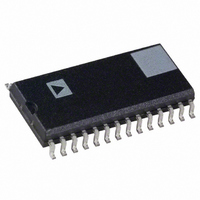
AD7244JRZ Analog Devices Inc, AD7244JRZ Datasheet - Page 7

AD7244JRZ
Manufacturer Part Number
AD7244JRZ
Description
IC DAC 14BIT LC2MOS DUAL 28SOIC
Manufacturer
Analog Devices Inc
Datasheet
1.AD7244JRZ.pdf
(12 pages)
Specifications of AD7244JRZ
Data Interface
Serial
Settling Time
4µs
Number Of Bits
14
Number Of Converters
2
Voltage Supply Source
Dual ±
Power Dissipation (max)
205mW
Operating Temperature
-40°C ~ 85°C
Mounting Type
Surface Mount
Package / Case
28-SOIC (7.5mm Width)
Resolution (bits)
14bit
Sampling Rate
250kSPS
Input Channel Type
Serial
Supply Current
27mA
Digital Ic Case Style
SOIC
No. Of Pins
28
Supply Voltage Range - Analog
± 4.75V To ± 5.25V
Rohs Compliant
Yes
Lead Free Status / RoHS Status
Lead free / RoHS Compliant
Available stocks
Company
Part Number
Manufacturer
Quantity
Price
Company:
Part Number:
AD7244JRZ
Manufacturer:
Analog Devices Inc
Quantity:
135
Part Number:
AD7244JRZ
Manufacturer:
ADI/亚德诺
Quantity:
20 000
REV. A
Output Amplifier
The outputs from each of the voltage-mode DACs are buffered
by a noninverting amplifier. The buffer amplifier is capable of
developing 3 V across a 2 k and 100 pF load to ground, and
can produce 6 V peak-to-peak sine wave signals to a frequency
of 20 kHz. The output is updated on the falling edge of the
respective LDAC input. The output voltage settling time, to
within 1/2 LSB of its final value, is typically less than 2 s for
the AD7242 and 2.5 s for the AD7244.
The small signal (200 mV p-p) bandwidth of the output buffer
amplifier is typically 1 MHz. The output noise from the
amplifier is low, with a figure of 30 nV/ Hz at a frequency of
1 kHz. The broadband noise from the amplifier exhibits a
typical peak-to-peak figure of 150 V for a 1 MHz output
bandwidth. Figure 4 shows a typical plot of noise spectral
density versus frequency for the output buffer amplifier and for
the on-chip reference (including and excluding the decoupling
components).
TRANSFER FUNCTION
The basic circuit configuration for the AD7242/AD7244 is
shown in Figure 5. Table I and Table II show the ideal input
code to output voltage relationship for the AD7242 and
AD7244 respectively. Input coding for the AD7242/AD7244 is
2s complement.
Figure 4. Noise Spectral Density vs. Frequency
Figure 5. Basic Connection Diagram
–7–
For the AD7242, the output voltage can be expressed in terms
of the input code, N, using the following relationship:
where –2048
For the AD7244, the output voltage can be expressed in terms
of the input code, N, using the following relationship:
where –8192
Table II. AD7244 Ideal Input/Output Code Table Code
Table I. AD7242 Ideal Input/Output Code Table Code
DAC Latch Contents
MSB
01 11 1111 1111
01 11 1111 1110
00 00 0000 0001
00 00 0000 0000
11 11 1111 1111
10 00 0000 0001
10 00 0000 0000
*Assuming REF IN = +3 V.
DAC Latch Contents
MSB
01 1111 1111 1111
01 1111 1111 1110
00 0000 0000 0001
00 0000 0000 0000
11 1111 1111 1111
10 0000 0000 0001
10 0000 0000 0000
*Assuming REF IN = +3 V.
N
N
+8191
+2047
V
LSB
LSB
V
OUT
OUT
2 N REF IN
2 N REF IN
16384
Analog Output, V
+2.998535 V
+2.99707 V
+0.001465 V
0 V
–0.001465 V
–2.998535 V
–3 V
Analog Output, V
+2.999634 V
+2.99268 V
+0.000366 V
0 V
–0.000366 V
–2.999634 V
–3 V
AD7242/AD7244
4096
OUT
OUT
*
*


