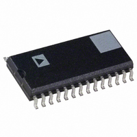
AD7244JRZ Analog Devices Inc, AD7244JRZ Datasheet - Page 5

AD7244JRZ
Manufacturer Part Number
AD7244JRZ
Description
IC DAC 14BIT LC2MOS DUAL 28SOIC
Manufacturer
Analog Devices Inc
Datasheet
1.AD7244JRZ.pdf
(12 pages)
Specifications of AD7244JRZ
Data Interface
Serial
Settling Time
4µs
Number Of Bits
14
Number Of Converters
2
Voltage Supply Source
Dual ±
Power Dissipation (max)
205mW
Operating Temperature
-40°C ~ 85°C
Mounting Type
Surface Mount
Package / Case
28-SOIC (7.5mm Width)
Resolution (bits)
14bit
Sampling Rate
250kSPS
Input Channel Type
Serial
Supply Current
27mA
Digital Ic Case Style
SOIC
No. Of Pins
28
Supply Voltage Range - Analog
± 4.75V To ± 5.25V
Rohs Compliant
Yes
Lead Free Status / RoHS Status
Lead free / RoHS Compliant
Available stocks
Company
Part Number
Manufacturer
Quantity
Price
Company:
Part Number:
AD7244JRZ
Manufacturer:
Analog Devices Inc
Quantity:
135
Part Number:
AD7244JRZ
Manufacturer:
ADI/亚德诺
Quantity:
20 000
REV. A
DIP
Pin No.
1
2
3
4
5
6
7
8
9
10
11
12
13
14
15
16
17
18
19
20
21
22
23
24
Mnemonic
LDACA
TFSA
DTA
TCLKA
DGND
TP1
V
AGND
V
V
TP2
REF INB
LDACB
TFSB
DTB
TCLKB
DGND
TP3
V
AGND
V
V
REF OUT
REF INA
DD
OUTB
SS
DD
OUTA
SS
Description
Load DAC, Logic Input. A new word is transferred into DAC Latch A from input Latch A on the fall-
ing edge of this signal. If LDACA is hard-wired low, data is transferred from input Latch A to DAC
Latch A on the sixteenth falling edge of TCLKA after TFSA goes low.
Transmit Frame Synchronization, Logic Input. This is a frame or synchronization signal for DACA
data with serial data expected after the falling edge of this signal.
Transmit Data, Logic Input. This is the data input which is used in conjunction with TFSA and
TCLKA to transfer serial data to input Latch A.
Transmit Clock, Logic Input. Serial data bits for DACA are latched on the falling edge of TCLKA
when TFSA is low.
Digital Ground. Both DGND pins for the device must be tied together at the device.
Test Pin 1. Used when testing the device. Do not connect anything to this pin.
Positive Power Supply, 5 V
Analog Ground. Both AGND pins for the device must be tied together at the device.
Analog Output Voltage from DACB. This output comes from a buffer amplifier. The range is bipolar,
Negative Power Supply, –5 V
Test Pin 2. Used when testing the device. Do not connect anything to this pin.
DACB Voltage Reference Input. The voltage reference for DACB is applied to this pin. It is internally
buffered before being applied to DACB. The nominal reference voltage for correct operation of the
AD7242/AD7244 is 3 V.
Load DAC, Logic Input. A new word is transferred into DAC Latch B from input Latch B on the fall-
ing edge of this signal. If LDACB is hard-wired low, data is transferred from input Latch B to DAC
Latch B on the sixteenth falling edge of TCLKB after TFSB goes low.
Transmit Frame Synchronization, Logic Input. This is a frame or synchronization signal for DACB
data with serial data expected after the falling edge of this signal.
Transmit Data, Logic Input. This is the data input used in conjunction with TFSB and TCLKB to
transfer serial data to input Latch B.
Transmit Clock, Logic Input. Serial data bits for DACB are latched on the falling edge of TCLKB
when TFSB is low.
Digital Ground. Both DGND pins for the device must be tied together at the device.
Test Pin 3. Used when testing the device. Do not connect anything to this pin.
Positive Power Supply, 5 V
Analog Ground. Both AGND pins for the device must be tied together at the device.
Analog Output Voltage from DACA. This output comes from a buffer amplifier. The range is bipolar,
Negative Power Supply, –5 V
Voltage Reference Output. To operate the DACs with this internal reference, REF OUT should be
connected to both REF INA and REF INB. The external load capability of the reference is 500 A.
DACA Voltage Reference Input. The voltage reference for DACA is applied to this pin. It is internally
buffered before being applied to DACA. The nominal reference voltage for correct operation of the
AD7242/AD7244 is 3 V.
3 V with REF INB = +3 V.
3 V with REF INA = +3 V.
AD7242/AD7244 PIN FUNCTION DESCRIPTION
5%. Both V
5%. Both V
5%. Both V
5%. Both V
–5–
DD
DD
SS
SS
pins for the device must be tied together at the device.
pins for the device must be tied together at the device.
pins for the device must be tied together at the device.
pins for the device must be tied together at the device.
AD7242/AD7244


