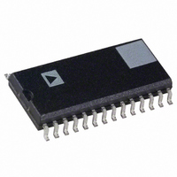
AD7244JRZ Analog Devices Inc, AD7244JRZ Datasheet - Page 8

AD7244JRZ
Manufacturer Part Number
AD7244JRZ
Description
IC DAC 14BIT LC2MOS DUAL 28SOIC
Manufacturer
Analog Devices Inc
Datasheet
1.AD7244JRZ.pdf
(12 pages)
Specifications of AD7244JRZ
Data Interface
Serial
Settling Time
4µs
Number Of Bits
14
Number Of Converters
2
Voltage Supply Source
Dual ±
Power Dissipation (max)
205mW
Operating Temperature
-40°C ~ 85°C
Mounting Type
Surface Mount
Package / Case
28-SOIC (7.5mm Width)
Resolution (bits)
14bit
Sampling Rate
250kSPS
Input Channel Type
Serial
Supply Current
27mA
Digital Ic Case Style
SOIC
No. Of Pins
28
Supply Voltage Range - Analog
± 4.75V To ± 5.25V
Rohs Compliant
Yes
Lead Free Status / RoHS Status
Lead free / RoHS Compliant
Available stocks
Company
Part Number
Manufacturer
Quantity
Price
Company:
Part Number:
AD7244JRZ
Manufacturer:
Analog Devices Inc
Quantity:
135
Part Number:
AD7244JRZ
Manufacturer:
ADI/亚德诺
Quantity:
20 000
AD7242/AD7244
TIMING AND CONTROL
Communication with the AD7242/AD7244 is via six serial logic
inputs. These consist of separate serial clocks, word framing and
data lines for each DAC. DAC updating is controlled by two
digital inputs: LDACA for updating V
updating V
the microprocessor by an external timer when precise updating
intervals are required. Alternatively, the LDACA and LDACB
inputs can be driven from a decoded address bus allowing the
microprocessor control over DAC updating as well as data
communication to the AD7242/AD7244 input latches.
The AD7242/AD7244 contains two latches per DAC, an input
latch and a DAC latch. Data must be loaded to the input latch
under the control of TCLKA, TFSA and DTA for input Latch
A and TCLKB, TFSB and DTB for input Latch B. Data is then
transferred from input Latch A to DAC Latch A under the control
of the LDACA signal, while LDACB controls the loading of DAC
Latch B from input Latch B. Only the data held in the DAC
latches determines the analog outputs of the AD7242/AD7244.
Data is loaded to the input latches under control of the respec-
tive TCLK, TFS and DT signals. The AD7242/AD7244
expects a 16-bit stream of serial data on its DT inputs. Data
must be valid on the falling edge of TCLK. The TFS input
provides the frame synchronization signal that tells the AD7242/
AD7244 that valid serial data will be available on the DT input
for the next 16 falling edges of TCLK. Figure 6 shows the
OUTB
. These inputs can be asserted independently of
OUTA
Figure 6. AD7242/AD7244 Timing Diagram
and LDACB for
–8–
timing diagram for operation of either of the two serial input
ports on the part.
Although 16 bits of data are clocked into the input latch, only
12 bits are transferred into the DAC latch for the AD7242 and
14 bits are transferred for the AD7244. Therefore, 4 bits in the
AD7242 data stream and 2 bits in the AD7244 data stream are
don’t cares since their value does not affect the DAC latch data.
The bit positions are the don’t cares followed by the DAC data
starting with the MSB (see Figure 6).
The respective LDAC signals control the transfer of data to the
respective DAC latches. Normally, data is loaded to the DAC
latch on the falling edge of LDAC. However, if LDAC is held
low, serial data is loaded to the DAC latch on the sixteenth
falling edge of TCLK. If LDAC goes low during the loading of
serial data to the input latch, no DAC latch update takes place
on the falling edge of LDAC. If LDAC stays low until the serial
transfer is completed, then the update takes place on the sixteenth
falling edge of TCLK. If LDAC returns high before the serial
data transfer is completed, no DAC latch update takes place.
If seventeen or more TCLK edges occur while TFS is low, the
seventeenth (and beyond) clock edges are ignored, i.e., no
further data is clocked into the input latch after the sixteenth
TCLK edge following a falling edge on TFS.
REV. A


