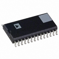
AD7244JRZ Analog Devices Inc, AD7244JRZ Datasheet - Page 3

AD7244JRZ
Manufacturer Part Number
AD7244JRZ
Description
IC DAC 14BIT LC2MOS DUAL 28SOIC
Manufacturer
Analog Devices Inc
Datasheet
1.AD7244JRZ.pdf
(12 pages)
Specifications of AD7244JRZ
Data Interface
Serial
Settling Time
4µs
Number Of Bits
14
Number Of Converters
2
Voltage Supply Source
Dual ±
Power Dissipation (max)
205mW
Operating Temperature
-40°C ~ 85°C
Mounting Type
Surface Mount
Package / Case
28-SOIC (7.5mm Width)
Resolution (bits)
14bit
Sampling Rate
250kSPS
Input Channel Type
Serial
Supply Current
27mA
Digital Ic Case Style
SOIC
No. Of Pins
28
Supply Voltage Range - Analog
± 4.75V To ± 5.25V
Rohs Compliant
Yes
Lead Free Status / RoHS Status
Lead free / RoHS Compliant
Available stocks
Company
Part Number
Manufacturer
Quantity
Price
Company:
Part Number:
AD7244JRZ
Manufacturer:
Analog Devices Inc
Quantity:
135
Part Number:
AD7244JRZ
Manufacturer:
ADI/亚德诺
Quantity:
20 000
Parameter
DC ACCURACY
REFERENCE OUTPUT
REFERENCE INPUTS
LOGIC INPUTS
ANALOG OUTPUTS
AC CHARACTERISTICS
POWER REQUIREMENTS
NOTES
1
2
3
4
Specifications subject to change without notice.
REV. A
Temperature ranges are as follows: J Version: 0 C to +70 C; A Version: –40 C to +85 C; S Version: –55 C to +125 C.
Measured with respect to REF IN and includes bipolar offset error.
For capacitive loads greater than 50 pF, a series resistor is required (see Internal Reference section).
Sample tested @ +25 C to ensure compliance.
Resolution
Integral Nonlinearity
Differential Nonlinearity
Bipolar Zero Error
Positive Full-Scale Error
Negative Full-Scale Error
REF OUT @ +25 C
REF OUT Tempco
Reference Load Change
REF INA, REF INB Input Range
Input Current
(LDACA, LDACB, TFSA, TFSB,
TCLKA, TCLKB, DTA, DTB)
(V
Voltage Output Settling Time
Digital-to-Analog Glitch Impulse
Digital Feedthrough
Channel-to-Channel Isolation
V
V
I
I
Total Power Dissipation
DD
SS
DD
SS
T
( REF OUT vs. I)
Input High Voltage, V
Input Low Voltage, V
Input Current, I
Input Capacitance, C
Output Voltage Range
DC Output Impedance
Short Circuit Current
Positive Full-Scale Change
Negative Full-Scale Change
OUTA
MIN
, V
to T
OUTB
MAX
)
IN
IN
INL
INH
3
2
4
2
4
Model
AD7244JN
AD7244JR
AD7244AQ
AD7244SQ
3
NOTES
1
2
This grade will be available to /883B processing only.
To order MIL-STD-883, Class B, processed parts, add /883B to part number.
N = Plastic DIP; Q = Cerdip; R = Small Outline IC (SOIC).
Contact local sales office for military data sheet and availability.
J, A Versions
14
2.99/3.01
2.98/3.02
35
–1
2.85/3.15
1
2.4
0.8
10
0.1
20
4
4
10
2
110
+5
–5
27
15
195
2
1
10
10
10
3
10
1
3
AD7244
1
Temperature
Range
–40 C to +85 C
–40 C to +85 C
–40 C to +85 C
–55 C to +125 C
AD7244 ORDERING GUIDE
2.85/3.15
20
S Version
14
2.99/3.01
2.98/3.02
35
–1
1
2.4
0.8
10
0.1
4
4
10
2
110
+5
–5
28
15
205
2
1
10
10
10
3
10
1
–3–
Units
Bits
ppm/ C typ
mV max
V min/V max
V min
V max
pF max
mA typ
nV secs typ
nV secs typ
dB typ
V nom
mA max
mA max
mW max
LSB max
LSB max
LSB max
LSB max
LSB max
V min/V max
V min/V max
V nom
V nom
A max
A max
s max
s max
typ
Integral
Nonlinearity
2 LSB max
2 LSB max
2 LSB max
2 LSB max
3 V
DAC Code Change All 1s to All 0s
V
Typically 130 mW
Test Conditions/Comments
Guaranteed Monotonic
Reference Load Current Change (0 A–500 A)
V
V
V
Settling Time to Within 1/2 LSB of Final Value
Typically 2.5 s
Typically 2.5 s
Cumulative Current from the Two V
Cumulative Current from the Two V
DD
DD
IN
OUT
5% for Specified Performance
5% for Specified Performance
= 0 V to V
= 5 V
= 5 V
5%
= 10 kHz Sine Wave
Package
Option
N-24
R-28
Q-24
Q-24
5%
5%
DD
2
AD7242/AD7244
DD
SS
Pins
Pins


