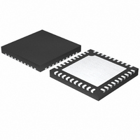
MAX1358BETL+ Maxim Integrated Products, MAX1358BETL+ Datasheet - Page 61

MAX1358BETL+
Manufacturer Part Number
MAX1358BETL+
Description
IC DAS 16BIT 40-TQFN
Manufacturer
Maxim Integrated Products
Type
Data Acquisition System (DAS)r
Datasheet
1.MAX1358BETL.pdf
(71 pages)
Specifications of MAX1358BETL+
Resolution (bits)
16 b
Sampling Rate (per Second)
21.84k
Data Interface
Serial
Voltage Supply Source
Analog and Digital
Voltage - Supply
1.8 V ~ 3.6 V
Operating Temperature
-40°C ~ 85°C
Mounting Type
Surface Mount
Package / Case
40-TQFN Exposed Pad
Number Of Converters
2
Resolution
16 bit
Interface Type
Serial (4-Wire, SPI, QSPI, Microwire)
Voltage Reference
1.25 V
Supply Voltage (max)
3.6 V
Supply Voltage (min)
1.8 V
Maximum Power Dissipation
2051.3 mW
Maximum Operating Temperature
+ 85 C
Mounting Style
SMD/SMT
Input Voltage
1.8 V to 3.6 V
Minimum Operating Temperature
- 40 C
Lead Free Status / RoHS Status
Lead free / RoHS Compliant
• With the SLEEP or SLEEP function deasserted on
• With the SLEEP or SLEEP function deasserted,
• With the SLEEP or SLEEP function deasserted, the
A wake-up event, such as an assertion of a UPIO con-
figured as WU or a time-of-day alarm causes the
MAX1358B to exit sleep mode, if in sleep mode. A
wake-up event in normal mode results only in a wake-up
event being recorded in the STATUS register.
The RESET output pulls low for any one of the following
cases: power-on reset, DV
RSTE = 0, watchdog timer expires, crystal oscillator is
attached, and 32kHz clock not ready.
The RESET output can be turned off through the RSTE
bit in the PS_VMONS register, causing DV
ply voltage events to issue an interrupt or poll through
the LDVD status bit. This allows brownout detection
µCs that operate with DV
UPIO outputs can be driven to AV
with separate AV
charge-pump doubler by setting CPE = 0 in the
PS_VMONS register, and connect the system’s analog
supply to AV
drive to CPOUT results in AV
16-Bit, Data-Acquisition System with ADC, DACs,
Figure 20. ADC Unipolar Transfer Function
UPIOs, RTC, Voltage Monitors, and Temp Sensor
UPIO, clear the SHDN bit by writing to the normal-
mode register address control byte.
assert WU or WU (wake-up) function on UPIO.
day alarm triggers.
1111 1111 1111 1111
1111 1111 1111 1110
1111 1111 1111 1101
1111 1111 1111 1100
0000 0000 0000 0011
0000 0000 0000 0010
0000 0000 0000 0001
0000 0000 0000 0000
Driving UPIO Outputs to AV
DD
0
1 LSB =
and CPOUT. Setting UPIO outputs to
DD
1
______________________________________________________________________________________
2
(GAIN x 65,536)
and DV
3
V
REF
DD
INPUT VOLTAGE (LSB)
FULL-SCALE TRANSITION
< 1.8V.
DD
DD
V
REF
DD
-referenced logic levels.
/GAIN
supplies. Disable the
DD
monitor trips and
levels in systems
65,533
DD
DD
Wake-Up
65,535
low sup-
Levels
RESET
The AV
ADC by reversing the normal input and reference sig-
nals. The REF voltage is applied to one multiplexer
input, and AGND is selected in the other. The AV
signal is then switched in as the ADC reference voltage
and a conversion is performed. The AV
then be calculated directly as:
where V
is the PGA gain before the ADC, and N is the ADC
result. Note the AV
gained-up REF voltage (AV
measurement must be done in unipolar mode.
Figure 21. ADC Bipolar Transfer Function
Figure 22. DAC Unipolar Output Circuit
0111 1111 1111 1111
0111 1111 1111 1110
0111 1111 1111 1101
0000 0000 0000 0001
0000 0000 0000 0000
1111 1111 1111 1111
1000 0000 0000 0010
1000 0000 0000 0001
1000 0000 0000 0000
DD
REF
REF
V
supply voltage can be measured with the
AVDD
is the reference voltage for the ADC, Gain
-32,768
MAX1358B
1 LSB =
DAC A
DAC B
Supply Voltage Measurement
= (V
DD
-32,766
V
(GAIN x 65,536)
REF
REF
voltage must be greater than the
/GAIN
V
REF
INPUT VOLTAGE (LSB)
x Gain x 65,536)/N
-1
x 2
DD
0
> V
+1
REF
FBA
FBB
V
REF
+32,765
/GAIN
DD
x Gain). This
OUTA
OUTB
value can
+32,767
DD
61


