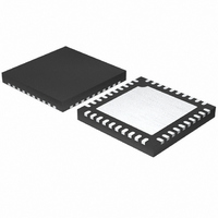
MAX1358BETL+ Maxim Integrated Products, MAX1358BETL+ Datasheet - Page 59

MAX1358BETL+
Manufacturer Part Number
MAX1358BETL+
Description
IC DAS 16BIT 40-TQFN
Manufacturer
Maxim Integrated Products
Type
Data Acquisition System (DAS)r
Datasheet
1.MAX1358BETL.pdf
(71 pages)
Specifications of MAX1358BETL+
Resolution (bits)
16 b
Sampling Rate (per Second)
21.84k
Data Interface
Serial
Voltage Supply Source
Analog and Digital
Voltage - Supply
1.8 V ~ 3.6 V
Operating Temperature
-40°C ~ 85°C
Mounting Type
Surface Mount
Package / Case
40-TQFN Exposed Pad
Number Of Converters
2
Resolution
16 bit
Interface Type
Serial (4-Wire, SPI, QSPI, Microwire)
Voltage Reference
1.25 V
Supply Voltage (max)
3.6 V
Supply Voltage (min)
1.8 V
Maximum Power Dissipation
2051.3 mW
Maximum Operating Temperature
+ 85 C
Mounting Style
SMD/SMT
Input Voltage
1.8 V to 3.6 V
Minimum Operating Temperature
- 40 C
Lead Free Status / RoHS Status
Lead free / RoHS Compliant
ALD: Alarm (day) status bit. ALD = 1 when the value
programmed in ASEC<19:0> in the AL_DAY register
matches SEC<19:0> in the RTC register. Clear the ALD
bit by reading the STATUS register or by disabling the
day alarm (ADE = 0). The power-on default is 0.
UPR<4:1>: User-programmable I/O rising-edge status
bits. UPR_ = 1 indicates a rising edge on the respec-
tive UPIO_ pin has occurred. Clear UPR_ by reading
the STATUS register. Rising edges are detected inde-
pendent of UPIO_ configuration, providing the ability to
capture and record rising input (e.g., WU) or output
(e.g., PWM) edge events on the UPIO_. Set the appro-
priate mask to determine if the edge will generate an
interrupt on INT. If the UPIO_ is configured as an out-
put, INT provides confirmation that an intended rising
edge output occurred and has reached the desired
DV
nally). The power-on default is 0.
UPF<4:1>: User-programmable I/O falling-edge status
bit. UPF_ = 1 indicates a falling edge on the respective
UPIO_ has occurred. Clear UPF_ by reading the
STATUS register. Falling edges are detected indepen-
dent of UPIO_ configuration, providing the ability to cap-
ture and record falling input (e.g., WU) or output (e.g.,
PWM) edge events on the UPIO_. Set the appropriate
mask to determine if that edge should generate an inter-
rupt on the INT pin. If the UPIO is configured as an out-
put, INT provides confirmation that an intended falling
edge output occurred at the pin and it reached the
desired DGND level. The power-on default is 0.
The internal digital filter does not provide rejection
close to the harmonics of the modulator sample fre-
quency. However, due to high oversampling ratios in
the MAX1358B, these bands typically occupy a small
fraction of the spectrum and most broadband noise is
filtered. Therefore, the analog filtering requirements in
front of the MAX1358B are considerably reduced com-
pared to a conventional converter with no on-chip filter-
ing. In addition, because the device’s common-mode
rejection (60dB) extends out to several kHz, the com-
mon-mode noise susceptibility in this frequency range
is substantially reduced.
Depending on the application, provide filtering prior to the
MAX1358B to eliminate unwanted frequencies the digital
filter does not reject. Providing additional filtering in some
applications ensures that differential noise signals outside
the frequency band of interest do not saturate the analog
modulator.
16-Bit, Data-Acquisition System with ADC, DACs,
UPIOs, RTC, Voltage Monitors, and Temp Sensor
DD
or CPOUT level (i.e., was not loaded down exter-
Applications Information
______________________________________________________________________________________
Analog Filtering
When placing passive components in front of the
MAX1358B, ensure a low enough source impedance to
prevent introducing gain errors to the system. This con-
figuration significantly limits the amount of passive anti-
aliasing filtering that can be applied in front of the
MAX1358B. See Table 3 for acceptable source imped-
ances.
After a power-on reset, the DV
enabled and all UPIOs are configured as inputs with
pullups enabled. The internal oscillators are enabled and
are output at CLK and CLK32K once the DV
supervisor is cleared and the subsequent timeout period
has expired. All interrupts are masked except CRDY.
Figure 19 illustrates the timing of various signals during
initial power-up, sleep mode, and wake-up events. The
ADC, charge pump, internal reference, op amp(s), DAC,
and switches are disabled after power-up.
Two power modes are available for the MAX1358B:
sleep and normal mode. In sleep mode, all functional
blocks are powered down except the serial interface,
data registers, internal bandgap, wake-up circuitry (if
enabled), DV
the 32kHz oscillator (if enabled), which remain active.
See Table 15 for details of the sleep-mode and normal-
mode power states of the various internal blocks.
Each analog block can be shut down individually
through its respective control register with the excep-
tion of the bandgap reference.
Sleep mode is entered one of three ways:
• Writing to the SLEEP register address. The result is
• Asserting the SLEEP or SLEEP function on a UPIO
• Asserting the SHDN bit by writing SLP = 1 in the
Entering sleep mode is an OR function of the UPIO or
SHDN bit. Before entering sleep mode, configure the
normal mode conditions.
Exit sleep mode and enter normal mode by one of the
following methods:
• With the SHDN bit = 0, deassert the SLEEP or
the SHDN bit is set to 1.
(SLEEP takes precedence over software writes or
wake-up events). The SHDN bit is unaffected.
SLEEP_CFG register.
SLEEP function on UPIO, only if SLEEP or SLEEP
function is used for entering sleep mode.
DD
voltage supervisor (if enabled), and
Power-On Reset or Power-Up
DD
voltage supervisor is
Power Modes
Sleep Mode
DD
voltage
59


