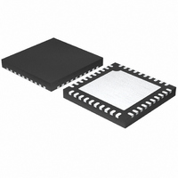
MAX1358BETL+ Maxim Integrated Products, MAX1358BETL+ Datasheet - Page 34

MAX1358BETL+
Manufacturer Part Number
MAX1358BETL+
Description
IC DAS 16BIT 40-TQFN
Manufacturer
Maxim Integrated Products
Type
Data Acquisition System (DAS)r
Datasheet
1.MAX1358BETL.pdf
(71 pages)
Specifications of MAX1358BETL+
Resolution (bits)
16 b
Sampling Rate (per Second)
21.84k
Data Interface
Serial
Voltage Supply Source
Analog and Digital
Voltage - Supply
1.8 V ~ 3.6 V
Operating Temperature
-40°C ~ 85°C
Mounting Type
Surface Mount
Package / Case
40-TQFN Exposed Pad
Number Of Converters
2
Resolution
16 bit
Interface Type
Serial (4-Wire, SPI, QSPI, Microwire)
Voltage Reference
1.25 V
Supply Voltage (max)
3.6 V
Supply Voltage (min)
1.8 V
Maximum Power Dissipation
2051.3 mW
Maximum Operating Temperature
+ 85 C
Mounting Style
SMD/SMT
Input Voltage
1.8 V to 3.6 V
Minimum Operating Temperature
- 40 C
Lead Free Status / RoHS Status
Lead free / RoHS Compliant
16-Bit, Data-Acquisition System with ADC, DACs,
UPIOs, RTC, Voltage Monitors, and Temp Sensor
The MAX1358B provides two uncommitted SPDT switch-
es. Each switch has a typical 35Ω on-resistance. Control
the switches through the SW_CTRL register, the PWM
output, and/or a UPIO port configured to control the
switches (UPIO1–UPIO4_CTRL register).
A single 8-bit PWM is available for various system tasks
such as LCD bias control, sensor bias voltage trim,
buzzer drive, and duty-cycled sleep-mode power-con-
trol schemes. PWM input clock sources include the
4.9512MHz FLL output, the 32kHz clock, and frequen-
cy-divided versions of each. Although most µCs have
built-in PWM functions, the MAX1358B PWM is more
flexible by allowing the UPIO outputs to be driven to
DV
For duty-cycled power-control schemes, use the
32kHz-derived input clock. The PWM output is avail-
able independent of µC power state. The FLL is typical-
ly disabled in sleep-override mode.
34
Single-Pole/Double-Throw (SPDT) Switches
DD
______________________________________________________________________________________
or regulated CPOUT logic-high voltage levels.
Pulse-Width Modulator (PWM)
The MAX1358B features a 4-wire serial interface con-
sisting of a chip select (CS), serial clock (SCLK), data
in (DIN), and data out (DOUT). CS must be low to allow
data to be clocked into or out of the device. DOUT is
high impedance while CS is high. The data is clocked
in at DIN on the rising edge of SCLK. Data is clocked
out at DOUT on the falling edge of SCLK. The serial
interface is compatible with SPI modes CPOL = 0,
CPHA = 0 and CPOL = 1, CPHA = 1. A write operation
to the MAX1358B takes effect on the last rising edge of
SCLK. If CS goes high before the complete transfer, the
write is ignored. Every data transfer is initiated by the
command byte. The command byte consists of a start
bit (MSB), R/W bit, and 6 address bits. The start bit
must be 1 to perform data transfers to the device.
Zeros clocked in are ignored. For SPI pass-through
mode, see the UPIO_SPI Register section. An address
byte identifies each register. Table 4 shows the com-
plete register address map for this family of DAS.
Figures 14, 15, and 16 provide timing diagrams for
read and write commands.
Serial Interface


