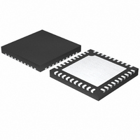
MAX1358BETL+ Maxim Integrated Products, MAX1358BETL+ Datasheet - Page 12

MAX1358BETL+
Manufacturer Part Number
MAX1358BETL+
Description
IC DAS 16BIT 40-TQFN
Manufacturer
Maxim Integrated Products
Type
Data Acquisition System (DAS)r
Datasheet
1.MAX1358BETL.pdf
(71 pages)
Specifications of MAX1358BETL+
Resolution (bits)
16 b
Sampling Rate (per Second)
21.84k
Data Interface
Serial
Voltage Supply Source
Analog and Digital
Voltage - Supply
1.8 V ~ 3.6 V
Operating Temperature
-40°C ~ 85°C
Mounting Type
Surface Mount
Package / Case
40-TQFN Exposed Pad
Number Of Converters
2
Resolution
16 bit
Interface Type
Serial (4-Wire, SPI, QSPI, Microwire)
Voltage Reference
1.25 V
Supply Voltage (max)
3.6 V
Supply Voltage (min)
1.8 V
Maximum Power Dissipation
2051.3 mW
Maximum Operating Temperature
+ 85 C
Mounting Style
SMD/SMT
Input Voltage
1.8 V to 3.6 V
Minimum Operating Temperature
- 40 C
Lead Free Status / RoHS Status
Lead free / RoHS Compliant
16-Bit, Data-Acquisition System with ADC, DACs,
UPIOs, RTC, Voltage Monitors, and Temp Sensor
TIMING CHARACTERISTICS (Figures 1 and 19)
(AV
10µF between CF+ and CF-, T
12
Note 16: The delay for the sleep voltage monitor output, RESET, to go high after V
Note 17: FLLE is gated by an AND function with three inputs—the external RESET signal, the internal DV
Note 18: If FLLE = 0, the internal signal CRDY is not generated by the FLL block and INT or INT is deasserted.
Note 19: CRDY is used as an interrupt signal to inform the µC that the high-frequency clock has started. Only valid if FLLE = 1.
Note 20: t
Note 21: t
SCLK Operating Frequency
SCLK Cycle Time
SCLK Pulse-Width High
SCLK Pulse-Width Low
DIN to SCLK Setup
DIN to SCLK Hold
SCLK Fall to DOUT Valid
CS Fall to DOUT Enable
CS Rise to DOUT Disable
CS to SCLK Rise Setup
CS to SCLK Rise Hold
DV
Wake-Up (WU) Pulse Width
Shutdown Delay
HFCLK Turn-On Time (Note 2)
CRDY to INT Delay
HFCLK Disable Delay
SHDN Assertion Delay
DD
DD
______________________________________________________________________________________
= DV
Monitor Timeout Period
driven by the startup of the 32kHz oscillator.
external SHDN signal. The time delay is timed from the internal LOV
whichever happens later. HFCLK always starts in the low state.
PARAMETER
DFOF
DPD
DD
is greater than the HFCLK delay to clean up before losing power.
= +1.8V to +3.6V, external V
gives the µC time to clean up and go into sleep-override mode properly.
A
= T
MIN
SYMBOL
t
f
t
to T
t
DFON
SCLK
t
t
t
t
DFOF
t
DSLP
t
t
t
t
t
CYC
t
t
t
t
CSS
CSH
DPU
DPD
DO
WU
DFI
CH
DH
CL
DS
DV
TR
MAX
REF
, unless otherwise noted. Typical values are at T
C
C
C
(Note 16)
Minimum pulse width required to detect a
wake-up event
The delay for SHDN to go high after a valid
wake-up event
The turn-on time for the high-frequency
clock and FLL (FLLE = 1) (Note 17)
If FLLE = 0, the turn-on time for the high-
frequency clock (Notes 7, 18)
The delay for CRDY to go low after the
HFCLK clock output has been enabled
(Note 19)
The delay after a shutdown command has
asserted and before HFCLK is disabled
(Note 20)
(Note 21)
= +1.25V, f
L
L
L
= 50pF, Figure 2
= 50pF, Figure 2
= 50pF, Figure 2
CLK32K
CONDITIONS
= 32.768kHz (external clock), C
DD
DD
going high or the external RESET going high,
rises above the reset threshold. This is largely
A
= +25°C.) (Note 1)
MIN
100
40
40
30
20
0
0
0
REG
DD
TYP
7.82
1.95
2.93
= 10µF, C
1.5
1
1
monitor output, and the
MAX
10
40
48
48
10
10
CPOUT
UNITS
= 10µF,
MHz
ms
ms
ms
ms
ns
ns
ns
ns
ns
ns
ns
ns
ns
ns
µs
µs
µs
s


