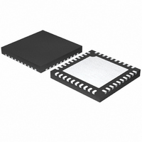
MAX1358BETL+ Maxim Integrated Products, MAX1358BETL+ Datasheet - Page 38

MAX1358BETL+
Manufacturer Part Number
MAX1358BETL+
Description
IC DAS 16BIT 40-TQFN
Manufacturer
Maxim Integrated Products
Type
Data Acquisition System (DAS)r
Datasheet
1.MAX1358BETL.pdf
(71 pages)
Specifications of MAX1358BETL+
Resolution (bits)
16 b
Sampling Rate (per Second)
21.84k
Data Interface
Serial
Voltage Supply Source
Analog and Digital
Voltage - Supply
1.8 V ~ 3.6 V
Operating Temperature
-40°C ~ 85°C
Mounting Type
Surface Mount
Package / Case
40-TQFN Exposed Pad
Number Of Converters
2
Resolution
16 bit
Interface Type
Serial (4-Wire, SPI, QSPI, Microwire)
Voltage Reference
1.25 V
Supply Voltage (max)
3.6 V
Supply Voltage (min)
1.8 V
Maximum Power Dissipation
2051.3 mW
Maximum Operating Temperature
+ 85 C
Mounting Style
SMD/SMT
Input Voltage
1.8 V to 3.6 V
Minimum Operating Temperature
- 40 C
Lead Free Status / RoHS Status
Lead free / RoHS Compliant
16-Bit, Data-Acquisition System with ADC, DACs,
UPIOs, RTC, Voltage Monitors, and Temp Sensor
Table 6a. Setting the ADC Conversion Rate*
Table 6b. Actual ADC Conversion Rates
*Calculate the ADC sampling rate using the following
equation:
where f
38
CONTINUOUS
CONVERSION
RATE (sps)
CONTINUOUS
CONVERSION
RATE (sps)
______________________________________________________________________________________
NOMINAL
200
240
400
477
10
40
50
60
HFCLK
200
240
400
477
10
40
50
60
f
= 4.9152MHz nominally.
S
CONVERSION
=
RATE (sps)
448
SINGLE
12.5
100
128
2.5
10
15
50
60
DECIMATION
×
decimation ratio
RATIO
f
1096
HFCLK
274
220
183
55
46
27
23
RATE2
0
0
0
0
1
1
1
1
RATE1
CONTINUOUS
CONVERSION
RATE (sps)
0
0
1
1
0
0
1
1
ACTUAL
199.48
238.51
406.35
477.02
10.01
40.04
49.87
59.95
RATE0
0
1
0
1
0
1
0
1
MODE<2:0>: Conversion-mode bits. These three bits
determine the type of conversion for the ADC as shown
in Table 7. When the ADC finishes an offset calibration
and/or gain calibration, the MODE<2:0> bits clear to 0
hex, the ADD bit in the STATUS register asserts, and
an interrupt asserts on INT (or UPIO_ if programmed as
DRDY) if MADD is unmasked. Perform a gain calibra-
tion after achieving the desired offset (calibrated or
not). If an offset and gain calibration are performed
together (MODE<2:0> = 7 hex), the offset calibration is
performed first followed by the gain calibration, and the
µC is interrupted by INT (or UPIO_ if programmed as
DRDY) if MADD is unmasked only upon completion of
both offset and gain calibration. After power-on or cali-
bration, the ADC does not begin conversions until initi-
ated by the user (see the ADCE and STRT bit
descriptions in this section and see the S bit descrip-
tions in the MUX Register section). See the GAIN CAL
Register and OFFSET CAL Register sections for details
on system calibration.
RATE<2:0>: ADC conversion-rate-setting bits. These
three bits set the conversion rate of the ADC as shown
in Table 6. The initial conversion requires four conver-
sion cycles for valid data, and subsequent conversions
require only one cycle (if CONT = 1). A full-scale input
change can require up to five cycles for valid data if
the digital filter is not reset with the STRT or S bit.
Table 7. Setting the ADC Conversion Mode
Normal
System Offset Calibration
System Gain Calibration
Normal
Normal
Self-Offset Calibration
Self-Gain Calibration
Self-Offset and Gain
Calibration
CONVERSION MODE
MODE2
0
0
0
0
1
1
1
1
MODE1
0
0
1
1
0
0
1
1
MODE0
0
1
0
1
0
1
0
1


