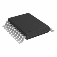
AD7927BRUZ Analog Devices Inc, AD7927BRUZ Datasheet - Page 9

AD7927BRUZ
Manufacturer Part Number
AD7927BRUZ
Description
IC ADC 12BIT 8CH 200KSPS 20TSSOP
Manufacturer
Analog Devices Inc
Specifications of AD7927BRUZ
Data Interface
DSP, MICROWIRE™, QSPI™, Serial, SPI™
Number Of Bits
12
Sampling Rate (per Second)
200k
Number Of Converters
1
Power Dissipation (max)
7.5mW
Voltage Supply Source
Single Supply
Operating Temperature
-40°C ~ 85°C
Mounting Type
Surface Mount
Package / Case
20-TSSOP (0.173", 4.40mm Width)
Resolution (bits)
12bit
Sampling Rate
200kSPS
Input Channel Type
Single Ended
Supply Voltage Range - Analog
2.7V To 5.25V
Supply Current
1.5mA
Number Of Elements
1
Resolution
12Bit
Architecture
SAR
Sample Rate
200KSPS
Input Polarity
Unipolar
Input Type
Voltage
Rated Input Volt
2.5/5V
Differential Input
No
Power Supply Requirement
Analog and Digital
Single Supply Voltage (typ)
3/5V
Single Supply Voltage (min)
2.7V
Single Supply Voltage (max)
5.25V
Dual Supply Voltage (typ)
Not RequiredV
Dual Supply Voltage (min)
Not RequiredV
Dual Supply Voltage (max)
Not RequiredV
Power Dissipation
7.5mW
Differential Linearity Error
-0.9LSB/1.5LSB
Integral Nonlinearity Error
±1LSB
Operating Temp Range
-40C to 85C
Operating Temperature Classification
Industrial
Mounting
Surface Mount
Pin Count
20
Package Type
TSSOP
Input Signal Type
Single-Ended
Lead Free Status / RoHS Status
Lead free / RoHS Compliant
For Use With
EVAL-AD7927CBZ - BOARD EVALUATION FOR AD7927
Lead Free Status / Rohs Status
Compliant
Available stocks
Company
Part Number
Manufacturer
Quantity
Price
Company:
Part Number:
AD7927BRUZ
Manufacturer:
ADI
Quantity:
1 000
Part Number:
AD7927BRUZ
Manufacturer:
ADI/亚德诺
Quantity:
20 000
Company:
Part Number:
AD7927BRUZ-REEL7
Manufacturer:
ADI
Quantity:
3
Company:
Part Number:
AD7927BRUZ-REEL7
Manufacturer:
ADI
Quantity:
1 000
Bit
11
10
9
8–6
5, 4
3
2
1
0
CONTROL REGISTER
The Control Register on the AD7927 is a 12-bit, write-only register. Data is loaded from the DIN pin of the AD7927 on the falling
edge of SCLK. The data is transferred on the DIN line at the same time that the conversion result is read from the part. The data
transferred on the DIN line corresponds to the AD7927 configuration for the next conversion. This requires 16 serial clocks for every
data transfer. Only the information provided on the first 12 falling clock edges (after CS falling edge) is loaded to the Control Register.
MSB denotes the first bit in the data stream. The bit functions are outlined in Table I.
REV. 0
MSB
WRITE
–0.2
–0.4
–0.6
–0.8
–1.0
Mnemonic
WRITE
SEQ
DONTC
ADD2–ADD0 These three address bits are loaded at the end of the present conversion and select which analog input channel
PM1, PM0
SHADOW
DONTC
RANGE
CODING
1.0
0.8
0.6
0.4
0.2
0
0
AV
TEMP = 25 C
DD
SEQ
512
= V
DRIVE
1024
TPC 6. Typical INL
= 5V
DONTC ADD2
Comment
The value written to this bit of the Control Register determines whether the following 11 bits will be loaded
to the Control Register. If this bit is a 1, the following 11 bits will be written to the Control Register; if it is
a 0, then the remaining 11 bits are not loaded to the Control Register and it remains unchanged.
The SEQ bit in the Control Register is used in conjunction with the SHADOW bit to control the use of the
sequencer function and access the Shadow Register. (See Table IV.)
Don’t Care
is to be converted in the next serial transfer, or they may select the final channel in a consecutive sequence
as described in Table IV. The selected input channel is decoded as shown in Table II. The address bits
corresponding to the conversion result are also output on DOUT prior to the 12 bits of data. (See the Serial
Interface section.) The next channel to be converted on will be selected by the mux on the 14th SCLK
falling edge.
Power Management Bits. These two bits decode the mode of operation of the AD7927 as shown in Table III.
The SHADOW bit in the Control Register is used in conjunction with the SEQ bit to control the use of the
sequencer function and access the Shadow Register. (See Table IV.)
Don’t Care
This bit selects the analog input range to be used on the AD7927. If it is set to 0, the analog input range
will extend from 0 V to 2 ¥ REF
(for the next conversion). For the 0 V to 2 ¥ REF
This bit selects the type of output coding the AD7927 will use for the conversion result. If this bit is set to
0, the output coding for the part will be twos complement. If this bit is set to 1, the output coding from the
part will be straight binary (for the next conversion).
1536
CODE
2048
2560
3072
ADD1
Table I. Control Register Bit Functions
3584
4096
ADD0 PM1
IN
. If it is set to 1, the analog input range will extend from 0 V to REF
–9–
PM0 SHADOW DONTC
IN
–0.2
–0.4
–0.6
–0.8
–1.0
range, AV
1.0
0.8
0.6
0.4
0.2
0
0
AV
TEMP = 25 C
DD
512
= V
DD
DRIVE
1024
TPC 7. Typical DNL
= 4.75 V to 5.25 V.
= 5V
1536
CODE
2048
2560
RANGE
3072
AD7927
3584
LSB
CODING
4096
IN


