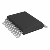
AD7927BRUZ Analog Devices Inc, AD7927BRUZ Datasheet - Page 18

AD7927BRUZ
Manufacturer Part Number
AD7927BRUZ
Description
IC ADC 12BIT 8CH 200KSPS 20TSSOP
Manufacturer
Analog Devices Inc
Specifications of AD7927BRUZ
Data Interface
DSP, MICROWIRE™, QSPI™, Serial, SPI™
Number Of Bits
12
Sampling Rate (per Second)
200k
Number Of Converters
1
Power Dissipation (max)
7.5mW
Voltage Supply Source
Single Supply
Operating Temperature
-40°C ~ 85°C
Mounting Type
Surface Mount
Package / Case
20-TSSOP (0.173", 4.40mm Width)
Resolution (bits)
12bit
Sampling Rate
200kSPS
Input Channel Type
Single Ended
Supply Voltage Range - Analog
2.7V To 5.25V
Supply Current
1.5mA
Number Of Elements
1
Resolution
12Bit
Architecture
SAR
Sample Rate
200KSPS
Input Polarity
Unipolar
Input Type
Voltage
Rated Input Volt
2.5/5V
Differential Input
No
Power Supply Requirement
Analog and Digital
Single Supply Voltage (typ)
3/5V
Single Supply Voltage (min)
2.7V
Single Supply Voltage (max)
5.25V
Dual Supply Voltage (typ)
Not RequiredV
Dual Supply Voltage (min)
Not RequiredV
Dual Supply Voltage (max)
Not RequiredV
Power Dissipation
7.5mW
Differential Linearity Error
-0.9LSB/1.5LSB
Integral Nonlinearity Error
±1LSB
Operating Temp Range
-40C to 85C
Operating Temperature Classification
Industrial
Mounting
Surface Mount
Pin Count
20
Package Type
TSSOP
Input Signal Type
Single-Ended
Lead Free Status / RoHS Status
Lead free / RoHS Compliant
For Use With
EVAL-AD7927CBZ - BOARD EVALUATION FOR AD7927
Lead Free Status / Rohs Status
Compliant
Available stocks
Company
Part Number
Manufacturer
Quantity
Price
Company:
Part Number:
AD7927BRUZ
Manufacturer:
ADI
Quantity:
1 000
Part Number:
AD7927BRUZ
Manufacturer:
ADI/亚德诺
Quantity:
20 000
Company:
Part Number:
AD7927BRUZ-REEL7
Manufacturer:
ADI
Quantity:
3
Company:
Part Number:
AD7927BRUZ-REEL7
Manufacturer:
ADI
Quantity:
1 000
AD7927
that when writing to the AD7927 between these valid conversions,
the DOUT line will not be driven during the extra write operation,
as shown in Figure 19.
It is critical that an extra write operation as outlined above is
never issued between valid conversions when the AD7927 is
executing through a sequence function, as the falling edge of CS
in the extra write would move the mux on to the next channel in
the sequence. This means when the next valid conversion takes
place, a channel result would have been missed.
MICROPROCESSOR INTERFACING
The serial interface on the AD7927 allows the part to be directly
connected to a range of many different microprocessors. This
section explains how to interface the AD7927 with some of the
more common microcontroller and DSP serial interface protocols.
AD7927 to TMS320C541
The serial interface on the TMS320C541 uses a continuous serial
clock and frame synchronization signals to synchronize the data
transfer operations with peripheral devices like the AD7927. The
CS input allows easy interfacing between the TMS320C541 and
the AD7927 without any glue logic required. The serial port of
the TMS320C541 is set up to operate in burst mode with internal
CLKX0 (TX serial clock on serial port 0) and FSX0 (TX frame
sync from serial port 0). The serial port control register (SPC)
must have the following setup: FO = 0, FSM = 1, MCM = 1, and
TXM = 1. The connection diagram is shown in Figure 20. It
should be noted that for signal processing applications, it is impera-
tive that the frame synchronization signal from the TMS320C541
provides equidistant sampling. The V
takes the same supply voltage as that of the TMS320C541. This
allows the ADC to operate at a higher voltage than the serial
interface, i.e., TMS320C541, if necessary.
*ADDITIONAL PINS REMOVED FOR CLARITY
AD7927
Figure 20. Interfacing to the TMS320C541
DOUT
SCLK
V
*
DRIVE
DIN
CS
DOUT
SCLK
DIN
CS
DRIVE
1
VALID DATA
pin of the AD7927
Figure 19. General Timing Diagram
CLKX
CLKR
DR
DT
FSX
FSR
TMS320C541*
16
V
DD
t
CYCLE
5 s MIN
–18–
AD7927 to ADSP-21xx
The ADSP-21xx family of DSPs are interfaced directly to the
AD7927 without any glue logic required. The V
the AD7927 takes the same supply voltage as that of the
ADSP-218x. This allows the ADC to operate at a higher voltage
than the serial interface, i.e., ADSP-218x, if necessary.
The SPORT0 Control Register should be set up as follows:
The connection diagram is shown in Figure 21. The ADSP-218x
has the TFS and RFS of the SPORT tied together, with TFS set
as an output and RFS set as an input. The DSP operates in Alter-
nate Framing Mode and the SPORT Control Register is set up as
described. The frame synchronization signal generated on the TFS
is tied to CS, and as with all signal processing applications equi-
distant sampling is necessary. However, in this example the timer
interrupt is used to control the sampling rate of the ADC, and
under certain conditions equidistant sampling may not be achieved.
1
TFSW = RFSW = 1, Alternate Framing
INVRFS = INVTFS = 1, Active Low Frame Signal
DTYPE = 00, Right Justify Data
SLEN = 1111, 16-Bit Data-Words
ISCLK = 1, Internal Serial Clock
TFSR = RFSR = 1, Frame Every Word
IRFS = 0
ITFS = 1
POWER-UP
*ADDITIONAL PINS REMOVED FOR CLARITY
AD7927
V
DRIVE
16
Figure 21. Interfacing to the ADSP-218x
DOUT
SCLK
*
DIN
CS
1
VALID DATA
t
QUIET
MIN
16
DR
RFS
TFS
DT
SCLK
V
ADSP-218x*
DD
DRIVE
pin of
REV. 0


