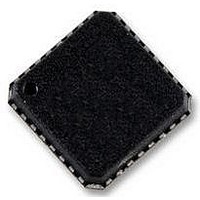
AD7194BCPZ Analog Devices Inc, AD7194BCPZ Datasheet - Page 43

AD7194BCPZ
Manufacturer Part Number
AD7194BCPZ
Description
IC ADC 24BIT SPI 4.8K 32-LFCSP
Manufacturer
Analog Devices Inc
Datasheet
1.AD7194BCPZ.pdf
(56 pages)
Specifications of AD7194BCPZ
Data Interface
DSP, MICROWIRE™, QSPI™, Serial, SPI™
Number Of Bits
24
Sampling Rate (per Second)
4.8k
Number Of Converters
1
Voltage Supply Source
Analog and Digital
Operating Temperature
-40°C ~ 105°C
Mounting Type
Surface Mount
Package / Case
32-WFQFN, CSP Exposed Pad
Resolution (bits)
24bit
Input Channel Type
Pseudo Differential
Supply Voltage Range - Analogue
3V To 5.25V
Supply Voltage Range - Digital
2.7V To 5.25V
Supply
RoHS Compliant
Sampling Rate
4.8kSPS
Rohs Compliant
Yes
Lead Free Status / RoHS Status
Lead free / RoHS Compliant
Other names
AD7194BRUZ
AD7194BRUZ
AD7194BRUZ
Available stocks
Company
Part Number
Manufacturer
Quantity
Price
Part Number:
AD7194BCPZ
Manufacturer:
ADI/亚德诺
Quantity:
20 000
Simultaneous 50 Hz and 60 Hz rejection is obtained when
FS[9:0] is set to 480 (master clock = 4.92 MHz), as shown in
Figure 41. The output data rate is 10 Hz when zero latency is
disabled and 3.3 Hz when zero latency is enabled. The sinc
filter has rejection of 100 dB minimum at 50 Hz ± 1 Hz and
60 Hz ± 1 Hz.
Simultaneous 50 Hz/60 Hz rejection is also achieved using the
REJ60 bit in the mode register. When FS[9:0] is programmed to
96 and the REJ60 bit is set to 1, notches are placed at both 50 Hz
and 60 Hz for a stable 4.92 MHz master clock. Figure 42 shows
the frequency response of the sinc
Assuming a stable clock, the rejection at 50 Hz/60 Hz (±1 Hz)
is in excess of 67 dB minimum.
–100
–110
–120
–100
–120
–110
–10
–20
–30
–40
–50
–60
–70
–80
–90
–10
–20
–30
–40
–50
–60
–70
–80
–90
0
0
Figure 42. Sinc
0
0
Figure 41. Sinc
25
30
3
Filter Response (FS[9:0] = 96, REJ60 = 1)
50
3
Filter Response (FS[9:0] = 480)
FREQUENCY (Hz)
FREQUENCY (Hz)
60
3
75
filter with this configuration.
90
100
120
125
15
150
0
3
Rev. 0 | Page 43 of 56
CHOP ENABLED (SINC
With chop enabled, the ADC offset and offset drift are minimized.
The analog input pins are continuously swapped. With the
analog input pins connected in one direction, the settling time
of the sinc filter is allowed and a conversion is recorded. The
analog input pins are then inverted, and another settled conver-
sion is obtained. Subsequent conversions are averaged to
minimize the offset. This continuous swapping of the analog
input pins and the averaging of subsequent conversions means
that the offset drift is also minimized. With chop enabled, the
resolution increases by 0.5 bits.
Output Data Rate and Settling Time (Sinc
Enabled)
For the sinc
where:
f
f
FS[9:0] is the decimal equivalent of Bit FS9 to Bit FS0 in the
mode register.
The value of FS[9:0] can be varied from 1 to 1023. This results
in an output data rate of 1.17 Hz to 1200 Hz. The settling time is
equal to
Table 32 gives some examples of FS[9:0] values and the corres-
ponding output data rates and settling times.
Table 32. Examples of Output Data Rates and the
Corresponding Settling Time
FS[9:0]
96
80
ADC
CLK
is the master clock (4.92 MHz nominal).
is the output data rate.
f
t
ADC
SETTLE
= f
CHOP
= 2/f
CLK
Output Data Rate (Hz)
12.5
15
4
filter, the output data rate is equal to
/(4 × 1024 × FS[9:0])
ADC
MODULATOR
Figure 43. Chop Enabled
4
FILTER)
ADC
SINC
3
/SINC
4
Settling Time (ms)
160
133
POST FILTER
4
Chop
AD7194


