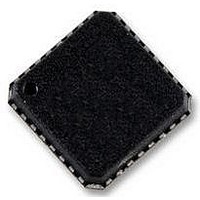
AD7194BCPZ Analog Devices Inc, AD7194BCPZ Datasheet - Page 10

AD7194BCPZ
Manufacturer Part Number
AD7194BCPZ
Description
IC ADC 24BIT SPI 4.8K 32-LFCSP
Manufacturer
Analog Devices Inc
Datasheet
1.AD7194BCPZ.pdf
(56 pages)
Specifications of AD7194BCPZ
Data Interface
DSP, MICROWIRE™, QSPI™, Serial, SPI™
Number Of Bits
24
Sampling Rate (per Second)
4.8k
Number Of Converters
1
Voltage Supply Source
Analog and Digital
Operating Temperature
-40°C ~ 105°C
Mounting Type
Surface Mount
Package / Case
32-WFQFN, CSP Exposed Pad
Resolution (bits)
24bit
Input Channel Type
Pseudo Differential
Supply Voltage Range - Analogue
3V To 5.25V
Supply Voltage Range - Digital
2.7V To 5.25V
Supply
RoHS Compliant
Sampling Rate
4.8kSPS
Rohs Compliant
Yes
Lead Free Status / RoHS Status
Lead free / RoHS Compliant
Other names
AD7194BRUZ
AD7194BRUZ
AD7194BRUZ
Available stocks
Company
Part Number
Manufacturer
Quantity
Price
Part Number:
AD7194BCPZ
Manufacturer:
ADI/亚德诺
Quantity:
20 000
AD7194
PIN CONFIGURATION AND FUNCTION DESCRIPTIONS
Table 5. Pin Function Descriptions
Pin No.
1
2
3
4
5
6
7
8
9
10
11
12
13
14
15
16
17
18
19
20
21
22
Mnemonic
AIN1/P3
AIN2/P2
AIN3/P1/REFIN2(+)
AIN4/P0/REFIN2(−)
AINCOM
AGND
AIN5
AIN6
AIN7
AIN8
AIN9
AIN10
AIN11
AIN12
AIN13
AIN14
REFIN1(+)
REFIN1(−)
AIN15
AIN16
AGND
DGND
Description
Analog Input/Digital Output Pin. This pin can function as an analog input pin. When the GP32EN bit is set
to 1, the pin functions as a general-purpose output bit referenced between AV
Analog Input/Digital Output Pin. This pin can function as an analog input pin. When the GP32EN bit is set
to 1, the pin functions as a general-purpose output bit referenced between AV
Analog Input/Digital Output Pin/Positive Reference Input. This pin functions as an analog input pin. When
the GP10EN bit is set to 1, the pin functions as a general-purpose output bit referenced between AV
AGND. When the REFSEL bit in the configuration register is set to 1, this pin functions as REFIN2(+). An
external reference can be applied between REFIN2(+) and REFIN2(−). REFIN2(+) can lie anywhere between
AV
Analog Input/Digital Output Pin/Positive Reference Input. This pin functions as an analog input pin. When
the GP10EN bit is set to 1, the pin functions as a general-purpose output bit referenced between AV
AGND. When the REFSEL bit in the configuration register is set to 1, this pin functions as REFIN2(−). An
external reference can be applied between REFIN2(+) and REFIN2(−). This reference input can lie anywhere
between AGND and AV
Analog Input AIN1 to Analog Input AIN16 are referenced to this input when the bit pseudo is set to 1.
Analog Ground Reference Point.
Analog Input Pin.
Analog Input Pin.
Analog Input Pin.
Analog Input Pin.
Analog Input Pin.
Analog Input Pin.
Analog Input Pin.
Analog Input Pin.
Analog Input Pin.
Analog Input Pin.
Positive Reference Input. An external reference can be applied between REFIN1(+) and REFIN1(−).
REFIN1(+) can lie anywhere between AV
REFIN1(−)), is AV
Negative Reference Input. This reference input can lie anywhere between AGND and AV
Analog Input Pin.
Analog Input Pin.
Analog Ground Reference Point.
Digital Ground Reference Point.
DD
and AGND + 1 V.
AIN3/P1/REFIN2(+)
AIN4/P0/REFIN2(–)
NOTES
1. NC = NO CONNECT.
2. CONNECT EXPOSED PAD TO AGND.
DD
, but the part functions with a reference from 1 V to AV
AINCOM
AIN1/P3
AIN2/P2
AGND
AIN5
AIN6
DD
Figure 5. Pin Configuration
− 1 V.
1
2
3
4
5
6
7
8
Rev. 0 | Page 10 of 56
(Not to Scale)
AD7194
TOP VIEW
DD
and AGND + 1 V. The nominal reference voltage, (REFIN1(+) −
24 DV
23 AV
22 DGND
21 AGND
20 AIN16
19 AIN15
18 REFIN1(–)
17 REFIN1(+)
DD
DD
DD
.
DD
DD
and AGND.
and AGND.
DD
− 1 V.
DD
DD
and
and


