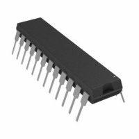
AD7870JNZ Analog Devices Inc, AD7870JNZ Datasheet - Page 5

AD7870JNZ
Manufacturer Part Number
AD7870JNZ
Description
IC ADC 12BIT LC2MOS 100KHZ 24DIP
Manufacturer
Analog Devices Inc
Datasheet
1.AD7870JNZ.pdf
(28 pages)
Specifications of AD7870JNZ
Data Interface
Serial, Parallel
Number Of Bits
12
Sampling Rate (per Second)
100k
Number Of Converters
1
Power Dissipation (max)
95mW
Voltage Supply Source
Dual ±
Operating Temperature
0°C ~ 70°C
Mounting Type
Through Hole
Package / Case
24-DIP (0.300", 7.62mm)
Resolution (bits)
12bit
Sampling Rate
100kSPS
Input Channel Type
Single Ended
Supply Voltage Range - Analog
± 4.75V To ± 5.25V
Supply Current
8mA
Number Of Elements
1
Resolution
12Bit
Architecture
SAR
Sample Rate
100KSPS
Input Polarity
Bipolar
Input Type
Voltage
Rated Input Volt
±3V
Differential Input
No
Power Supply Requirement
Dual
Single Supply Voltage (typ)
Not RequiredV
Single Supply Voltage (min)
Not RequiredV
Single Supply Voltage (max)
Not RequiredV
Dual Supply Voltage (typ)
±5V
Dual Supply Voltage (min)
±4.75V
Dual Supply Voltage (max)
±5.25V
Power Dissipation
95mW
Integral Nonlinearity Error
±0.5LSB(Typ)
Operating Temp Range
0C to 70C
Operating Temperature Classification
Commercial
Mounting
Through Hole
Pin Count
24
Package Type
PDIP
Input Signal Type
Single-Ended
Lead Free Status / RoHS Status
Lead free / RoHS Compliant
Lead Free Status / RoHS Status
Lead free / RoHS Compliant, Lead free / RoHS Compliant
Parameter
ANALOG INPUT
REFERENCE OUTPUT
LOGIC INPUTS
LOGIC OUTPUTS
CONVERSION TIME
POWER REQUIREMENTS
1
2
3
4
5
For the AD7875, the temperature range for the K and L versions is from 0°C to +70°C; for the B and C versions is−40°C to +85°C; and for the T version is −55°C to
+125°C. For the AD7876, the temperature range for the B and C versions is from −40°C to +85°C and for the T version is−55°C to +125°C.
Includes internal reference error and is calculated after unipolar offset error (AD7875) or bipolar zero error (AD7876) has been adjusted out. Full-scale error refers to
both positive and negative full-scale error for the AD7876.
Dynamic performance parameters are not tested on the AD7876, but these are typically the same as for the AD7875.
SNR calculation includes distortion and noise components.
Sample tested @ +25°C to ensure compliance.
AD7875 Input Voltage Range
AD7875 Input Current
AD7876 Input Voltage Range
AD7876 Input Current
REF OUT @ +25°C
REF OUT Tempco
Reference Load Sensitivity
Input High Voltage, V
Input Low Voltage, V
Input Current, I
Input Current (12/8/CLK Input Only)
Input Capacitance, C
Output High Voltage, V
Output Low Voltage, V
DB11–DB0
External Clock (f
Internal Clock
(ΔREF OUT/ΔI)
Floating-State Leakage Current
Floating-State Output
Capacitance
IN
CLK
5
= 2.5 MHz)
INL
IN
INH
5
OL
OH
K, B
0 to +5
500
±10
±600
2.99
3.01
±60
−1
2.4
0.8
±10
±10
10
4.0
0.4
10
15
8
6.5/9
AD7875/AD7876
As per AD7870
L, C
0 to +5
500
±10
±600
2.99
3.01
±35
−1
2.4
0.8
±10
±10
10
4.0
0.4
10
15
8
6.5/9
Rev. C | Page 5 of 28
T
0 to +5
500
±10
±600
2.99
3.01
±60
−1
2.4
0.8
±10
±10
10
4.0
0.4
10
15
8
6.5/9
1
Units
μA max
V
μA max
V min
V max
ppm/°C max
mV max
V min
V max
μA max
μA max
pF max
V min
V max
μA max
pF max
μs max
μs min/μs
max
V
Test Conditions/Comments
Typical tempco Is ±20 ppm/°C
Reference load current change (0 μA to 500 μA).
Reference load should not be changed during
conversion.
V
V
V
V
I
I
Refer to the power requirements in Table 1.
SOURCE
SINK
DD
DD
IN
IN
= 0 V to V
= V
= 5 V ± 5%
= 5 V ± 5%
= 1.6 mA
= 40 mA
SS
AD7870/AD7875/AD7876
to V
DD
DD


