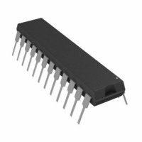
AD7870JNZ Analog Devices Inc, AD7870JNZ Datasheet - Page 11

AD7870JNZ
Manufacturer Part Number
AD7870JNZ
Description
IC ADC 12BIT LC2MOS 100KHZ 24DIP
Manufacturer
Analog Devices Inc
Datasheet
1.AD7870JNZ.pdf
(28 pages)
Specifications of AD7870JNZ
Data Interface
Serial, Parallel
Number Of Bits
12
Sampling Rate (per Second)
100k
Number Of Converters
1
Power Dissipation (max)
95mW
Voltage Supply Source
Dual ±
Operating Temperature
0°C ~ 70°C
Mounting Type
Through Hole
Package / Case
24-DIP (0.300", 7.62mm)
Resolution (bits)
12bit
Sampling Rate
100kSPS
Input Channel Type
Single Ended
Supply Voltage Range - Analog
± 4.75V To ± 5.25V
Supply Current
8mA
Number Of Elements
1
Resolution
12Bit
Architecture
SAR
Sample Rate
100KSPS
Input Polarity
Bipolar
Input Type
Voltage
Rated Input Volt
±3V
Differential Input
No
Power Supply Requirement
Dual
Single Supply Voltage (typ)
Not RequiredV
Single Supply Voltage (min)
Not RequiredV
Single Supply Voltage (max)
Not RequiredV
Dual Supply Voltage (typ)
±5V
Dual Supply Voltage (min)
±4.75V
Dual Supply Voltage (max)
±5.25V
Power Dissipation
95mW
Integral Nonlinearity Error
±0.5LSB(Typ)
Operating Temp Range
0C to 70C
Operating Temperature Classification
Commercial
Mounting
Through Hole
Pin Count
24
Package Type
PDIP
Input Signal Type
Single-Ended
Lead Free Status / RoHS Status
Lead free / RoHS Compliant
Lead Free Status / RoHS Status
Lead free / RoHS Compliant, Lead free / RoHS Compliant
CONVERTER DETAILS
The AD7870/AD7875/AD7876 is a complete 12-bit ADC,
requiring no external components apart from power supply
decoupling capacitors. It is comprised of a 12-bit successive
approximation ADC based on a fast settling voltage output
DAC, a high speed comparator and SAR, a track-and-hold
amplifier, a 3 V buried Zener reference, a clock oscillator,
and control logic.
INTERNAL REFERENCE
The AD7870/AD7875/AD7876 have on-chip temperature
compensated buried Zener reference that is factory trimmed
to 3 V ± 10 mV. Internally it provides both the DAC reference
and the dc bias required for bipolar operation (AD7870 and
AD7876). The reference output is available (REF OUT) and
capable of providing up to 500 μA to an external load.
The maximum recommended capacitance on REF OUT for
normal operation is 50 pF. If the reference is required for use
external to the ADC, it should be decoupled with a 200 Ω
resistor in series with a parallel combination of a 10 μF
tantalum capacitor and a 0.1 μF ceramic capacitor. These
decoupling components are required to remove voltage
spikes caused by the ADC’s internal operation.
The reference output voltage is 3 V. For applications using the
AD7875 or AD7876, a 5 V or 10 V reference may be required.
Figure 7 shows how to scale the 3 V REF OUT voltage to
provide either a 5 V or 10 V external reference.
INTERNAL 3V
REFERENCE
AD7870/AD7875/AD7876
Figure 7. Generating a 5 V or 10 V Reference
V
V
DD
SS
Figure 6. Reference Circuit
COMPENSATION
TEMPERATURE
AD7870/AD7875/AD7876
REF OUT
(3.9kΩ)
15kΩ
(9.1kΩ)
10kΩ
REF OUT
V
OUT
= 5V (10V)
Rev. C | Page 11 of 28
TRACK-AND-HOLD AMPLIFIER
The track-and-hold amplifier on the analog input of the
AD7870/AD7875/AD7876 allows the ADC to accurately
convert input frequencies to 12-bit accuracy. The input
bandwidth of the track-and-hold amplifier is much greater
than the Nyquist rate of the ADC even when the ADC is
operated at its maximum throughput rate. The 0.1 dB cutoff
frequency occurs typically at 500 kHz. The track-and-hold
amplifier acquires an input signal to 12-bit accuracy in less than
2 μs. The overall throughput rate is equal to the conversion time
plus the track-and-hold amplifier acquisition time. For a 2.5 MHz
input clock the throughput rate is 10 μs max.
The operation of the track-and-hold is essentially transparent
to the user. The track-and-hold amplifier goes from its tracking
mode to its hold mode at the start of conversion.
If the CONVST input is used to start conversion then the track
to hold transition occurs on the rising edge of CONVST . If CS
starts conversion, this transition occurs on the falling edge of CS .
ANALOG INPUT
The three parts differ from each other in the analog input
voltage range that they can handle. The AD7870 accepts ±3 V
input signals, the AD7876 accepts a ±10 V input range, while
the input range for the AD7875 is 0 V to +5 V.
Figure 8 shows the AD7870 analog input. The analog input
range is ±3 V into an input resistance of typically 15 kΩ. The
designed code transitions occur midway between successive
integer LSB values (that is, 1/2 LSB, 3/2 LSBs, 5/2 LSBs . . .
FS–3/2 LSBs). The output code is twos complement binary with
1 LSB = FS/4096 = 6 V/4096 = 1.46 mV. The ideal input/output
transfer function is shown in Figure 11.
The AD7876 analog input structure is shown in Figure 9. The
analog input range is ±10 V into an input resistance of typically
33 kΩ. As before, the designed code transitions occur midway
between successive integer LSB values. The output code is twos
complement with 1 LSB = FS/4096 = 20 V/4096 = 4.88 mV. The
ideal input/output transfer function is shown in Figure 11.
R
R
Figure 8. AD7970 Analog Input
TRACK-AND-HOLD
AD7870/AD7875/AD7876
AMPLIFIER
3V REFERENCE
TO INTERNAL
AD7870
COMPARATOR
TO INTERNAL


