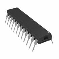
AD7870JNZ Analog Devices Inc, AD7870JNZ Datasheet - Page 20

AD7870JNZ
Manufacturer Part Number
AD7870JNZ
Description
IC ADC 12BIT LC2MOS 100KHZ 24DIP
Manufacturer
Analog Devices Inc
Datasheet
1.AD7870JNZ.pdf
(28 pages)
Specifications of AD7870JNZ
Data Interface
Serial, Parallel
Number Of Bits
12
Sampling Rate (per Second)
100k
Number Of Converters
1
Power Dissipation (max)
95mW
Voltage Supply Source
Dual ±
Operating Temperature
0°C ~ 70°C
Mounting Type
Through Hole
Package / Case
24-DIP (0.300", 7.62mm)
Resolution (bits)
12bit
Sampling Rate
100kSPS
Input Channel Type
Single Ended
Supply Voltage Range - Analog
± 4.75V To ± 5.25V
Supply Current
8mA
Number Of Elements
1
Resolution
12Bit
Architecture
SAR
Sample Rate
100KSPS
Input Polarity
Bipolar
Input Type
Voltage
Rated Input Volt
±3V
Differential Input
No
Power Supply Requirement
Dual
Single Supply Voltage (typ)
Not RequiredV
Single Supply Voltage (min)
Not RequiredV
Single Supply Voltage (max)
Not RequiredV
Dual Supply Voltage (typ)
±5V
Dual Supply Voltage (min)
±4.75V
Dual Supply Voltage (max)
±5.25V
Power Dissipation
95mW
Integral Nonlinearity Error
±0.5LSB(Typ)
Operating Temp Range
0C to 70C
Operating Temperature Classification
Commercial
Mounting
Through Hole
Pin Count
24
Package Type
PDIP
Input Signal Type
Single-Ended
Lead Free Status / RoHS Status
Lead free / RoHS Compliant
Lead Free Status / RoHS Status
Lead free / RoHS Compliant, Lead free / RoHS Compliant
AD7870/AD7875/AD7876
This is a two-byte read instruction. During the first read
operation BUSY , in conjunction with CS , forces the micro-
processor to WAIT for the ADC conversion. At the end of
conversion the ADC low byte (DB7 – DB0) is loaded into
D15 – D8 of the D0 register and the ADC high byte (DB15 –
DB7) is loaded into Bits D7 – D0 of the D0 register.
The following rotate instruction to the D0 register swaps the
high and low bytes to the correct format.
R0L = 8, D0.
Note that while executing the two-byte read instruction above,
WAIT states are inserted during the first read operation only
and not for the second.
SERIAL INTERFACING
Figure 26, Figure 27, Figure 28, and Figure 29 show the
AD7870/AD7875/AD7876 configured for serial interfacing. In
all four interfaces, the ADC is configured for Mode 1 operation.
The interfaces show a timer driving the CONVST input, but
this could be generated from a decoded address if required. The
SCLK, SDAT and SSTRB are open-drain outputs. If these are
required to drive capacitive loads in excess 35 pF, buffering is
recommended.
DSP56000 Serial Interface
Figure 26 shows a serial interface between the AD7870/AD7875/
AD7876, and the DSP56000. The interface arrangement is
two-wire with the ADC configured for noncontinuous clock
operation (12/ 8 /CLK = 0 V). The DSP56000 is configured
for normal mode asynchronous operation with gated clock.
It is also set up for a 16-bit word with SCK and SC1 as inputs
and the FSL control bit set to a 0. In this configuration, the
DSP56000 assumes valid data on the first falling edge of SCK.
Since the ADC provides valid data on this first edge, there is
no need for a strobe or framing pulse for the data. SCLK and
SDATA are gated off when the ADC is not performing a
1
2
ADDITIONAL PINS OMITTED FOR CLARITY.
RESISTOR AND CAPACITOR REQUIRED TO GUARANTEE
MC68008
DTACK
STRB
R/W
A15
D15
AS
A0
D0
Figure 25. MC68008 Byte Interface
ADDRESS BUS
EN
DECODE
R
ADDR
2
C
DATA BUS
A0
HBEN
CS
BUSY/INT
RD
12/8/CLK
CONVST
DB7
DB0
t
15 .
AD7870/
AD7875/
AD7876
1
Rev. C | Page 20 of 28
conversion. During conversion, data is valid on the SDATA
output of the ADC and is clocked into the receive data shift
register of the DSP56000. When this register has received
16 bits of data, it generates an internal interrupt on the
DSP56000 to read the data from the register.
The DSP56000 and AD7870/AD7875/AD7876 can also be
configured for continuous clock operation (12/ 8 /CLK = −5 V).
In this case, a strobe pulse is required by the DSP56000 to
indicate when data is valid. The SSTRB output of the ADC
is inverted and applied to the SC1 input of the DSP56000 to
provide this strobe pulse. All other conditions and connections
are the same as for gated clock operation.
NEC7720/77230 Serial Interface
A serial interface between the AD7870/AD7875/AD7876 and
the NEC7720 is shown in Figure 27. In the interface shown, the
ADC is configured for continuous clock operation. This can be
changed to a noncontinuous clock by simply tying the 12/ 8 /CLK
input of the ADC to 0 V with all other connections remaining
the same. The NEC7720 expects valid data on the rising edge of
its SCK input and therefore an inverter is required on the SCLK
output of the ADC. The NEC7720 is configured for a 16-bit
data word. Once the 16 bits of data have been received by the SI
register of the NEC7720, an internal interrupt is generated to
read the contents of the SI register.
The NEC77230 interface is similar to that just outlined for the
NEC7720. However, the clock input of the NEC77230 is SICLK.
Additionally, no inverter is required between the ADC SCLK
output and this SICLK input since the NEC77230 assumes data
is valid on the falling edge of SICLK.
1
ADDITIONAL PINS OMITTED FOR CLARITY.
1
µPD7720
ADDITIONAL PINS OMITTED FOR CLARITY.
DSP56000
SCLK
SIEN
SCK
SRD
SI
Figure 26. DSP56000 Serial Interface
4.7kΩ
Figure 27. NEC7720 Serial Interface
4.7kΩ
4.7kΩ
5V
+5V
2kΩ
TIMER
TIMER
2kΩ
–5V
CONVST
12/8/CLK
SCLK
SDATA
CONVST
12/8/CLK
SSTRB
SCLK
SDATA
AD7870/
AD7875/
AD7876
AD7870/
AD7875/
AD7876
1
1


