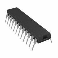
AD7870JNZ Analog Devices Inc, AD7870JNZ Datasheet - Page 19

AD7870JNZ
Manufacturer Part Number
AD7870JNZ
Description
IC ADC 12BIT LC2MOS 100KHZ 24DIP
Manufacturer
Analog Devices Inc
Datasheet
1.AD7870JNZ.pdf
(28 pages)
Specifications of AD7870JNZ
Data Interface
Serial, Parallel
Number Of Bits
12
Sampling Rate (per Second)
100k
Number Of Converters
1
Power Dissipation (max)
95mW
Voltage Supply Source
Dual ±
Operating Temperature
0°C ~ 70°C
Mounting Type
Through Hole
Package / Case
24-DIP (0.300", 7.62mm)
Resolution (bits)
12bit
Sampling Rate
100kSPS
Input Channel Type
Single Ended
Supply Voltage Range - Analog
± 4.75V To ± 5.25V
Supply Current
8mA
Number Of Elements
1
Resolution
12Bit
Architecture
SAR
Sample Rate
100KSPS
Input Polarity
Bipolar
Input Type
Voltage
Rated Input Volt
±3V
Differential Input
No
Power Supply Requirement
Dual
Single Supply Voltage (typ)
Not RequiredV
Single Supply Voltage (min)
Not RequiredV
Single Supply Voltage (max)
Not RequiredV
Dual Supply Voltage (typ)
±5V
Dual Supply Voltage (min)
±4.75V
Dual Supply Voltage (max)
±5.25V
Power Dissipation
95mW
Integral Nonlinearity Error
±0.5LSB(Typ)
Operating Temp Range
0C to 70C
Operating Temperature Classification
Commercial
Mounting
Through Hole
Pin Count
24
Package Type
PDIP
Input Signal Type
Single-Ended
Lead Free Status / RoHS Status
Lead free / RoHS Compliant
Lead Free Status / RoHS Status
Lead free / RoHS Compliant, Lead free / RoHS Compliant
MICROPROCESSOR INTERFACE
The AD7870/AD7875/AD7876 have a wide variety of
interfacing options. They offer two operating modes and
three data-output formats. Fast data access times allow
direct interfacing to most microprocessors including the
DSP processors.
PARALLEL READ INTERFACING
Figure 22, Figure 23, and Figure 24 show interfaces to the
ADSP-2100, TMS32010 and the TMS32020 DSP processors.
The ADC is operating in Mode 1, parallel read for all three
interfaces. An external timer controls conversion start asyn-
chronously to the microprocessor. At the end of each conversion
the ADC BUSY / INT interrupts the microprocessor. The
conversion result is read from the ADC with the following
instruction:
ADSP-2100: MR0 = DM(ADC)
TMS32010: IN D,ADC
TMS32020: IN D,ADC
MR0 = ADSP-2100 MR0 Register
D = Data Memory Address
ADC = AD7870/AD7875/AD7876 Address
Some applications may require that conversions be initiated by
the microprocessor rather than an external timer. One option
is to decode the CONVST signal from the address bus so that a
write operation to the ADC starts a conversion. Data is read at
the end of conversion as described earlier. Note: a read
operation must not be attempted during conversion.
1
ADDITIONAL PINS OMITTED FOR CLARITY.
ADSP-2100
DMA13
DMD15
DMRD
DMA0
DMD0
Figure 22. ADSP-2100 Parallel Interface
IRQn
DMS
ADDRESS BUS
EN
DECODE
ADDR
DATA BUS
TIMER
5V
CONVST
CS
12/8/CLK
BUSY/INT
RD
DB11
DB0
AD7870/
AD7875/
AD7876
1
Rev. C | Page 19 of 28
TWO-BYTE READ INTERFACING
68008 Interface
Figure 25 shows an 8-bit bus interface for the MC68008 micro-
processor. For this interface, the 12/ 8 /CLK input is tied to 0 V
and the DB11/HBEN pin is driven from the microprocessor
least significant address bit. Conversion start control is provided
by the microprocessor. In this interface example, a Move instruc-
tion from the ADC address both starts a conversion and reads
the conversion result.
MOVEW ADC,DO
ADC = AD7870/AD7875/AD7876 address
D0 = 68008 D0 register
1
1
ADDITIONAL PINS OMITTED FOR CLARITY.
ADDITIONAL PINS OMITTED FOR CLARITY.
TMS32010
TMS32020
STRB
Figure 23. TMS32010 Parallel Interface
Figure 24. TMS32020 Parallel Interface
MEN
INTn
DEN
R/W
PA2
PA0
D15
A15
D15
INT
D0
A0
D0
IS
ADDRESS BUS
ADDRESS BUS
AD7870/AD7875/AD7876
EN
EN
DECODE
DECODE
ADDR
ADDR
DATA BUS
DATA BUS
TIMER
TIMER
5V
5V
CONVST
CS
12/8/CLK
BUSY/INT
RD
DB11
DB0
CONVST
CS
12/8/CLK
BUSY/INT
RD
DB11
DB0
AD7870/
AD7875/
AD7876
AD7870/
AD7875/
AD7876
1
1


