AD7870JNZ Analog Devices Inc, AD7870JNZ Datasheet - Page 13

AD7870JNZ
Manufacturer Part Number
AD7870JNZ
Description
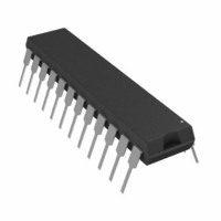
IC ADC 12BIT LC2MOS 100KHZ 24DIP
Manufacturer
Analog Devices Inc
Datasheet
1.AD7870JNZ.pdf
(28 pages)
Specifications of AD7870JNZ
Data Interface
Serial, Parallel
Number Of Bits
12
Sampling Rate (per Second)
100k
Number Of Converters
1
Power Dissipation (max)
95mW
Voltage Supply Source
Dual ±
Operating Temperature
0°C ~ 70°C
Mounting Type
Through Hole
Package / Case
24-DIP (0.300", 7.62mm)
Resolution (bits)
12bit
Sampling Rate
100kSPS
Input Channel Type
Single Ended
Supply Voltage Range - Analog
± 4.75V To ± 5.25V
Supply Current
8mA
Number Of Elements
1
Resolution
12Bit
Architecture
SAR
Sample Rate
100KSPS
Input Polarity
Bipolar
Input Type
Voltage
Rated Input Volt
±3V
Differential Input
No
Power Supply Requirement
Dual
Single Supply Voltage (typ)
Not RequiredV
Single Supply Voltage (min)
Not RequiredV
Single Supply Voltage (max)
Not RequiredV
Dual Supply Voltage (typ)
±5V
Dual Supply Voltage (min)
±4.75V
Dual Supply Voltage (max)
±5.25V
Power Dissipation
95mW
Integral Nonlinearity Error
±0.5LSB(Typ)
Operating Temp Range
0C to 70C
Operating Temperature Classification
Commercial
Mounting
Through Hole
Pin Count
24
Package Type
PDIP
Input Signal Type
Single-Ended
Lead Free Status / RoHS Status
Lead free / RoHS Compliant
Lead Free Status / RoHS Status
Lead free / RoHS Compliant, Lead free / RoHS Compliant
Positive Full-Scale Adjust
Apply a voltage of 2.9978 V (FS/2 − 3/2 LSBs) at V
until the ADC output code flickers between 0111 1111 1110 and
0111 1111 1111.
Negative Full-Scale Adjust
Apply a voltage of −2.9993 V (−FS/2 + 1/2 LSB) at V
R2 until the ADC output code flickers between 1000 0000 0000
and 1000 0000 0001.
OFFSET AND FULL-SCALE ADJUSTMENT—
AD7876
The offset and full-scale adjustment for the AD7876 is similar
to that just outlined for the AD7870. The trim procedure, for
those applications that do require adjustment, is as follows:
apply a voltage of −2.44 mV (−1/2 LSB) at V
amp offset voltage until the ADC output code flickers between
1111 1111 1111 and 0000 0000 0000. Full-scale error can be
adjusted at either the first code transition (ADC negative full
scale) or the last code transition (ADC positive full scale). The
trim procedure for both case is as described in the following
sections (see Figure 13).
1
V
ADDITIONAL PINS OMITTED FOR CLARITY.
1
Figure 13. Offset and Full-Scale Adjust Circuit
10kΩ
500Ω
10kΩ
R1
R2
R3
10kΩ
R5
10kΩ
R4
AGND
V
AD7876
AD7870/
AD7875/
IN
1
and adjust the op
1
1
. Adjust R2
1
and adjust
Rev. C | Page 13 of 28
Positive Full-Scale Adjust
Apply a voltage of 9.9927 V (FS/2 − 3/2 LSBs) at V
until the ADC output code flickers between 0111 1111 1110 and
0111 1111 1111.
Negative Full-Scale Adjust
Apply a voltage of −9.9976 V (FS/2 + 1/2 LSB) at V
R2 until the ADC output code flickers between 1000 0000 0000
and 1000 0000 0001.
OFFSET AND FULL-SCALE ADJUSTMENT—
AD7875
Similar to the AD7870, most of the DSP applications in which
the AD7875 is used do not require offset and full-scale
adjustment. For applications that do require adjustment, offset
error must be adjusted before full-scale (gain) error. This is
achieved by applying an input voltage of 0.61 mV (1/2 LSB) to
V
the ADC output code flickers between 0000 0000 0000 and
0000 0000 0001. For full-scale adjustment, apply an input
voltage of 4.9982 V (FS − 3/2 LSBs) to V
the ADC output code flickers between 1111 1111 1110 and
1111 1111 1111.
1
in Figure 13 and adjusting the op amp offset voltage until
AD7870/AD7875/AD7876
1
and adjust R2 until
1
1
. Adjust R2
and adjust


