MAXQ3180-RAN+ Maxim Integrated Products, MAXQ3180-RAN+ Datasheet - Page 24
MAXQ3180-RAN+
Manufacturer Part Number
MAXQ3180-RAN+
Description
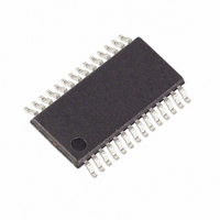
IC AFE POLYPHASE MULTI 28-TSSOP
Manufacturer
Maxim Integrated Products
Datasheet
1.MAXQ3180-RAN.pdf
(101 pages)
Specifications of MAXQ3180-RAN+
Number Of Channels
8
Power (watts)
35mW
Voltage - Supply, Analog
3.6V
Voltage - Supply, Digital
3.6V
Package / Case
28-TSSOP
For Use With
MAXQ3180-KIT - KIT EV REFRNC DSIGN FOR MAXQ3180
Lead Free Status / RoHS Status
Lead free / RoHS Compliant
Number Of Bits
-


Low-Power, Multifunction, Polyphase AFE
more bytes than are required by the current command,
the extra bytes are either ignored (if the MAXQ3180 is
busy processing the previous command) or are inter-
preted as the beginning of a new command. If the mas-
ter sends fewer bytes than are required by the current
command, the MAXQ3180 waits for SPI timeout, then
drops the transaction and resets the communication
channel. The duration of the timeout can be configured
through the COM_TIMO register.
Figures 5 and 6 show typical 2-byte reading and writing
transfers (without CRC byte).
Individual message bytes sent through the SPI are
processed in a software routine contained in the ROM
firmware. For this reason, it is necessary to provide a
delay between successive bytes. This byte spacing
must be no less than 400 system clocks to ensure that
the MAXQ3180 has a chance to read and process the
byte before the arrival of the next one.
Figure 5. Read SPI Transfer
Figure 6. Write SPI Transfer
24
______________________________________________________________________________________
SCLK
MOSI
MISO
SCLK
MOSI
MISO
SSEL
SSEL
00 01
10 01
0xC1
0xC1
Host Software Design
ADDRESS
ADDRESS
0xC2
0xC2
WRITING DATA TO MAXQ3180 THROUGH SPI INTERFACE
READING DATA FROM MAXQ3180 THROUGH SPI INTERFACE
NACK (0x4E)
ACK (0x41)
DATA LSB
DUMMY
To read any virtual power registers, the host must first
confirm that the DSPRDY bit of the IRQ_FLAG register
is set, which indicates the last DSP cycle has complet-
ed, then proceed to reading all the desired virtual
power registers. For best communication efficiency, it is
recommended to complete reading the virtual power
registers before reading other registers. Virtual power
register reads must be completed within 50% of DSP
cycle time, from the moment the DSPRDY bit is set. Do
not forget to clear the DSPRDY bit, otherwise, host soft-
ware is not able to detect the completion of the new
DSP cycle. The MAXQ3180 does not clear the bit; it
only sets the bit whenever a DSP cycle processing is
completed. Users can clear the bit directly after the
confirmation that the bit is set. Clearing the DSPRDY bit
does not affect the DSP processing. It is strongly rec-
ommended that CRC be enabled for both read and
write to achieve reliable communications.
ACK (0x41)
DATA MSB
ACK (0x41)
DUMMY
NACK (0x4E)
DATA LSB
DUMMY
DUMMY
ACK (0x41)
DATA MSB
DUMMY
DUMMY
Related parts for MAXQ3180-RAN+
Image
Part Number
Description
Manufacturer
Datasheet
Request
R

Part Number:
Description:
KIT EV REFRNC DSIGN FOR MAXQ3180
Manufacturer:
Maxim Integrated Products
Datasheet:

Part Number:
Description:
Low-power, Multifunction, Polyphase Afe
Manufacturer:
Maxim Integrated Products, Inc.
Datasheet:
Part Number:
Description:
MAX7528KCWPMaxim Integrated Products [CMOS Dual 8-Bit Buffered Multiplying DACs]
Manufacturer:
Maxim Integrated Products
Datasheet:
Part Number:
Description:
Single +5V, fully integrated, 1.25Gbps laser diode driver.
Manufacturer:
Maxim Integrated Products
Datasheet:
Part Number:
Description:
Single +5V, fully integrated, 155Mbps laser diode driver.
Manufacturer:
Maxim Integrated Products
Datasheet:
Part Number:
Description:
VRD11/VRD10, K8 Rev F 2/3/4-Phase PWM Controllers with Integrated Dual MOSFET Drivers
Manufacturer:
Maxim Integrated Products
Datasheet:
Part Number:
Description:
Highly Integrated Level 2 SMBus Battery Chargers
Manufacturer:
Maxim Integrated Products
Datasheet:
Part Number:
Description:
Current Monitor and Accumulator with Integrated Sense Resistor; ; Temperature Range: -40°C to +85°C
Manufacturer:
Maxim Integrated Products
Part Number:
Description:
TSSOP 14/A°/RS-485 Transceivers with Integrated 100O/120O Termination Resis
Manufacturer:
Maxim Integrated Products
Part Number:
Description:
TSSOP 14/A°/RS-485 Transceivers with Integrated 100O/120O Termination Resis
Manufacturer:
Maxim Integrated Products
Part Number:
Description:
QFN 16/A°/AC-DC and DC-DC Peak-Current-Mode Converters with Integrated Step
Manufacturer:
Maxim Integrated Products
Part Number:
Description:
TDFN/A/65V, 1A, 600KHZ, SYNCHRONOUS STEP-DOWN REGULATOR WITH INTEGRATED SWI
Manufacturer:
Maxim Integrated Products
Part Number:
Description:
Integrated Temperature Controller f
Manufacturer:
Maxim Integrated Products
Part Number:
Description:
SOT23-6/I°/45MHz to 650MHz, Integrated IF VCOs with Differential Output
Manufacturer:
Maxim Integrated Products
Part Number:
Description:
SOT23-6/I°/45MHz to 650MHz, Integrated IF VCOs with Differential Output
Manufacturer:
Maxim Integrated Products