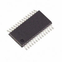
MAXQ3181-RAN+ Maxim Integrated Products, MAXQ3181-RAN+ Datasheet - Page 81

MAXQ3181-RAN+
Manufacturer Part Number
MAXQ3181-RAN+
Description
IC AFE POLYPHASE LO-PWR 28-TSSOP
Manufacturer
Maxim Integrated Products
Datasheet
1.MAXQ3181-RAN.pdf
(84 pages)
Specifications of MAXQ3181-RAN+
Number Of Channels
8
Power (watts)
35mW
Voltage - Supply, Analog
3.3V
Voltage - Supply, Digital
3.3V
Package / Case
28-TSSOP
Lead Free Status / RoHS Status
Lead free / RoHS Compliant
Number Of Bits
-
This register reports the RMS current of the neutral current
channel. The units are defined by the AMP_CC setting.
Table 7 shows the read-only virtual registers that acti-
vate special commands when read by the master.
Some commands return dummy values.
Careful PCB layout significantly minimizes noise on the
analog inputs, resulting in less noise on the digital I/O
that could cause improper operation. The use of multi-
layer boards is essential to allow the use of dedicated
power planes. The area under any digital components
should be a continuous ground plane if possible. Keep
any bypass capacitor leads short for best noise rejec-
tion and place the capacitors as close to the leads of
the devices as possible.
The MAXQ3181 must have separate ground areas for
the analog (AGND) and digital (DGND) portions, con-
nected together at a single point.
CMOS design guidelines for any semiconductor require
that no pin be taken above DVDD or below DGND.
Violation of this guideline can result in a hard failure
(damage to the silicon inside the device) or a soft fail-
Table 7. Virtual Registers That Activate Special Commands
ENTER LOWPM
ENTER STOP
EXIT LOWPM
RAWTEMP
UPD_SFR
UPD_MIR
DSPVER
NAME
Low-Power, Active Energy, Polyphase AFE
Applications Information
ADDRESS
______________________________________________________________________________________
0xA00
0xC00
0xC01
0xC02
0xC03
0xC04
0x900
RMS Current, Neutral (I.N) (0x840)
Grounds and Bypassing
Reading this register copies the mirror registers (R_ADCF, R_ADCRATE,
R_ADCACQ, R_SPICF) into hardware SFR registers. The read returns dummy data.
Reading this register copies hardware SFR registers into mirror registers (R_ADCF,
R_ADCRATE, R_ADCACQ, R_SPICF). The read returns dummy data.
Reading this register returns the DSP firmware version number.
Reading this register initiates the sampling and averaging of two internal
temperature readings. The result in internal temperature units is read from this
register LSB first. Use the following equation to convert a raw temperature reading to
Celsius: T[c] = T[raw] x TempFactor - 273.15
where TempFactor is a value to be determined by calibration. Note that the final
value may be slightly higher than ambient due to internal die heating.
Reading this register places the device into Stop Mode.
Reading this register places the device into LOWPM Mode.
Reading this register exits LOWPM Mode.
Special Commands
Neutral Current
DESCRIPTION
ure (unintentional modification of memory contents).
Voltage spikes above or below the device’s absolute
maximum ratings can potentially cause a devastating
IC latchup.
Microcontrollers commonly experience negative volt-
age spikes through either their power pins or general-
purpose I/O pins. Negative voltage spikes on power
pins are especially problematic as they directly couple
to the internal power buses. Devices such as keypads
can conduct electrostatic discharges directly into the
microcontroller and seriously damage the device.
System designers must protect components against
these transients that can corrupt system memory.
To reduce the possibility of coupling noise into the
microcontroller, the system should be designed with a
crystal or oscillator in a metal case that is grounded to
the digital plane. Doing so reduces the susceptibility of
the design to fast transient noise.
Because the MAXQ3181 is designed for use in systems
where high voltages are present, care must be taken to
route all signal paths, both analog and digital, as far
away as possible from the high-voltage components.
It is possible to construct more elaborate metering
designs using multiple MAXQ3181 devices. This can be
accomplished by using a single SPI bus to connect all
Specific Design Considerations for
MAXQ3181-Based Systems
LENGTH
(BYTES)
DATA
1
1
2
2
1
1
1
81


